
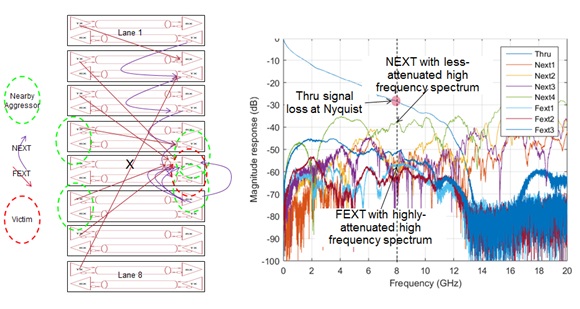
Figure 7: NEXT and FEXT example for an eight- lLane system
In most high-speed receivers, a continuous time linear equalizer (CTLE) is used to offer high-pass filtering to flatten signal spectrum of the signal seen at the data samplers to undo the low-pass effect of the channel. This enhances channel output signal spectrum of the desired signal around Nyquist, but it also enhances the signal spectrum of the NEXT (that has less relative attenuated high frequency spectrum) around Nyquist frequency.
Receiver design needs to have configurability in CTLE so that in low XTLK system, with XTLK detected by suitable algorithms, it can open up CTLE high frequency boost range for sufficient equalization. This is done in CTLE with wide bandwidth to preserve CTLE group delay behavior that aids in improved CTLE adaptation behavior. This strategy will be CTLE heavy and light in DFE utilization.
On the other hand, if excess XTLK is detected, then the CTLE high-frequency boost needs to be limited to minimize NEXT spectrum amplification around Nyquist frequency, and the bandwidth needs to be reduced so that CTLE does not amplify out-of-band NEXT spectrum. This strategy will be light in CTLE contribution and heavy in DFE utilization without amplifying undesired XTLK. This configuration will distort CTLE group delay behavior around Nyquist frequency, and proper steps needs to be taken to preserve the desired adaptation algorithm behavior. There are various techniques to sense XTLK level in a system; the explanation of those algorithms are beyond the scope of this paper.
Introduction to Inner and Outer Loop Equalization for System Level Optimization
Classical lane-by-lane SerDes transceiver optimization is system agnostic. A SerDes optimizes the far-end partner transmitter and its own local receiver on a per lane basis. It pays no attention to its neighboring lane. Such lane-by-lane SerDes transceiver equalization is called inner-loop equalization as shown in Figure 8. A system agnostic inner equalization may result in excess margin for lanes with shorter traces, while lanes with the longer traces may be performance limited, all within a single link. In such a scenario, at least one weakest PCIe lane in a PCIe link will be a single-point fail source.

Figure 8: Classical inner equalization loop does not optimize cross lane performance
A system-agnostic lane-by-lane optimization is acceptable for lower data rate applications. However, at PCIe Gen4 data rates with spec limit insertion loss that approaches 30dB and without significant XTLK floor reduction, the PCIe Gen4 inner-loop equalization approach will be challenged to meet the desired system target BER performance. Unlike in other standards, PCIe Gen4 does not have any forward error correction (FEC) protection. Fortunately, PCIe Gen4 standardized a “Lane Margin” feature allowing a host to detect the operating EYE margin of the repeaters or an end device at the normal L0 operating state [1]. The standardization of lane margin opens the door for many innovative system-level optimization methodologies. We address one application of the PCIe Gen4 Lane Margin feature to trade EYE margin between high margin lane and margin starved lanes through adjusting the transmitter amplitude, slew rate, and pre/post cursor of aggressor lanes shown in Figure 9 using an outer loop equalization scheme as shown in Figure 10.

Figure 9: Cross lane Transmitter transmitter control using outer- loop equalization
The outer-loop equalization helps XTLK-sensitive lanes with longer traces by adjusting the TX amplitude, or the slew rate, or the TX pre/post emphasis of lanes with shorter traces appropriately. This, in turn, reduces the XTLK floor in the system and helps the operating EYE margin of more stressed lanes as shown in Figure 10.
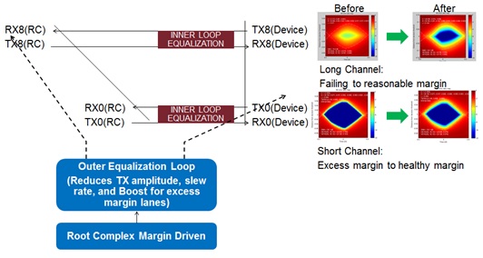
Figure 10: Lane margin assisted outer loop equalization
Before the outer loop equalization, the long-trace EYE margin was low, and the short-trace EYE margin was excessive. The outer-loop equalization detects the current state of the lane operating EYE margin using PCIe standardized scheme. The host instructs short trace lane(s) to increase the rise/fall time on both ends of the lane to reduce high frequency contents in the signal spectrum beyond Nyquist frequency. Then the host instructs the short trace lane(s) to reduce the transmitter amplitude on both ends using PCIe defined vendor specific messaging understood by both sides until long trace lane(s) operating margin improves and short trace lane(s) still maintain healthy operating margin. As a last resort, the short trace de-emphasis can also be adjusted to reduce overall system XTLK floor by reducing the transmitter output signal energy in the system and at the same time allowing its link partner receiver not to apply excess CTLE high frequency boost.
The flow diagram of the inner and outer equalization loop is presented in Figure 11. Initially, the system XTLK level is sensed using known algorithms on a per Lane basis. In a high XTLK environment, the Lane optimization is configured for a DFE heavy optimization scheme. In a low XTLK environment, the Lane optimization is configured for a CTLE heavy optimization scheme. Using conventional equalization methods, each lane will be optimized using back-channel adaptation by a receiver at each end of the link in conjunction with its link partner transmitter [12]. This level of equalization is overall system performance agnostic.

Figure 11: Inner and outer equalization loop sequencing
After initial lane-by-lane equalization, host-directed cross-lane optimization is performed using the PCIe Gen4 margin scheme. A host will identify excess margin lanes and margin starved lanes. Then, host-controlled outer equalization will direct host and device-side transmitters to adjust the transmitter launch amplitude, boost, and slew rate, such that excess-margin lanes will give up some margin and margin-starved lanes gain reasonable operating margin. The idea is to adjust the TX amplitude, boost, and slew rate to minimize the overall system XTLK contribution from high-margin lanes to help out margin-starved lanes gain sufficient operating margin due to reduced system impairment floor obtained through margin-assisted outer equalization loop.
A qualitative view of such an iterative outer-loop equalization scheme is presented in Figure 12 using the optimization flow shown in Figure 11. The classical inner loop equalization scheme reconfigures the receiver at each lane and performs lane-based inner-loop equalization to optimize each lane. It then transitions to L0 normal operating state in LTSSM and performs lane-by-lane margining to determine EYE margin of each lane. If all lanes have good operating margin, the outer equalization loop ends. If low and high margin lane is detected, then it instructs the high-margin lane to reduce its amplitude on both side of the lane.
This process will reduce system XTLK floor: Perform PCIe Lane margin in all lanes again. Repeat the lane margin and transmitter adjustment process until stressed lane EYE margin becomes acceptable without degrading the EYE margin of the good lane below the acceptable margin threshold. In case a balanced system performance is not reached, the outer-loop equalization cycles through the transmitter slew rate and de-emphasis adjustment. The order of transmitter parameter control is implementation specific or specific to a system need. Ideally, one would try adjusting the slew rate first, then adjust the amplitude, and then adjust the de-emphasis of the transmitter. A qualitative view of the stages of EYE balancing through the outer loop equalization is presented in Figure 12.

Figure 12: Long and short channel operating EYE margin balancing with outer equalization loop
Outer loop equalization implementation model using lane margin
The lane margining commands and responses introduced in the PCI Express Gen4 Base Specification include a vendor-defined command and response that can be used to control outer-loop equalization. The relevant portion of the Margining Commands and Corresponding Responses Table presented in the PCI Express Gen4 Base Specification is shown in Table 1.
Table 1: Vendor-defined Margin Command as presented in the PCIe Gen4 Base Specification
|
Command |
Response |
||||
|
Margin Command |
Margin Type [2:0] |
Valid Receiver Number(s) [2:0] |
Margin Payload [7:0] |
Margin Type [2:0] |
Margin Payload [7:0] |
|
Vendor Defined |
101b |
001b through 101b |
Vendor Defined |
101b |
Vendor Defined |
In the above table, the valid receiver number field is interpreted as shown below. Refer back to Figure 1 to see the relative locations of the transmitters and receivers within a link that optionally includes retimers. The value of Cmd[2:0] from Table 2 determines whether the ultimate target of a command is a receiver or a transmitter.
|
Encoding |
Receiver |
Transmitter |
|
001b |
Rx(A) |
Tx(B) |
|
010b |
Rx(B) |
Tx(C) |
|
011b |
Rx(C) |
Tx(D) |
|
100b |
Rx(D) |
Tx(E) |
|
101b |
Rx(E) |
Tx(F) |
For outer-loop equalization, the vendor-defined entry is defined shown in Table 2.
Table 2: Vendor-defined margin command for outer loop equalization
|
Command Payload Bit Definition |
Description |
Response Payload Bit Definition |
Description |
|---|---|---|---|
|
Payload[7:5] = Cmd[2:0] |
111b = Tx Amplitude 110b = Tx Slew Rate 101b = Pre Emphasis 100b = Post Emphasis 011b, 010b = Reserved 001b = Perform Rx Adaptation 000b = No Command |
Payload[7:5] = Status[2:0] |
Status[2:0] = 011b = NAK 010b = In Progress 001b = Setup 000b = Idle/Finished |
|
Payload[4] = Increase |
Specifies whether to increase or decrease the selected attribute. When Cmd[2:0] is 100b through 111b, 0b = Decrease 1b = Increase Otherwise, set to 0b |
Payload[4] = MaxValue |
1b = Maximum value (in positive or negative direction) reached 0b = Maximum value not reached |
|
Payload[3:0] = Amt[3:0] |
Specifies amount of increase/decrease for Tx Amplitude, Tx Slew Rate, Pre Emphasis, or Post Emphasis. Otherwise set to 0000b |
Payload[3:0] = Amt[3:0] |
When Cmd[2:0] is 100b through 111b, Response Payload[3:0] reflects Command Payload[3:0]. Otherwise, Response Payload[3:0] = 0000b |
- For commands: Tx Amplitude, Tx Slew Rate, Pre Emphasis, and Post Emphasis, the target of the command is a transmitter
- For command Rx Adaptation, the target of the command is a receiver
- When the amount of the specified increase or decrease takes the transmitter beyond its maximum supported value, the transmitter goes to its maximum value and reports that it has reached its maximum value in Response Payload[4].
- As with lane margining described in the PCIe Gen4 Base Specification, the host controls outer loop equalization of its own transmitters and receivers using PCI Configuration TLPs to write and read its lane margining at the receiver capability registers.
- As with lane margining described in the PCIe Gen4 Base Specification, the host controls outer loop equalization of the upstream port in the downstream component using PCI Configuration TLPs to write and read the downstream component lane margining at the receiver capability registers.
- As with lane margining described in the PCIe Gen4 Base Specification, the host controls outer loop equalization of retimer transmitters and receivers using Control SKP Ordered Sets.
Outer loop equalization proceeds as follows:
- System software determines which transmitter/receiver pairs within a link should be adjusted.
- System software sends commands that target the first set of transmitters (all at the same address, but on different lanes) to increase/decrease Tx Amplitude, Tx Slew Rate, Tx Pre Emphasis, and Tx Post Emphasis as needed.
- System software polls the status associated with the commands until all targeted transmitters return a NAK (indicating an error was encountered) or Idle/Finished status.
- System software then sends commands that target the receiver associated with the targeted transmitters. The receivers are commanded to perform Rx Adaptation.
- System software polls the status associated with the commands until all targeted transmitters return a NAK or Idle/Finished status.
- Steps 2 through 5 are repeated until system software is finished making adjustments.
- Then, system software performs lane margining to determine if there is adequate margin (refer to Figure 11). If the margin is now adequate, the process is complete. Otherwise, these steps can be repeated with remaining transmitter parameters.