
This paper introduces a concept of outer loop equalization for PCIe cross lane transmitter/receiver (transceiver) optimization using PCIe Gen4 Lane Margin capability introduced in the PCIe Gen4 specification [1]. Classical PCIe transceiver lane optimization, referred to here as inner-loop equalization, is done on a per-lane basis, without paying heed to the condition of the neighboring lanes. The neighboring lane may have excess operating margin and act as an aggressor against its neighbor. On the other hand, a neighboring lane could be a victim and could benefit if the excess operating margin of its aggressor neighboring lane could be reduced.
The goal of the introduction of outer-loop equalization is to provide a means to holistically and robustly optimize a system across all lanes, rather than being limited to individual lane optimization. We present a brief introduction to PCIe Gen4 lane margin, a best-mode-usage model of the scope of lane margin hardware/software capabilities, an application scenario of lane margin for outer loop equalization, and potential risks associated with lane margin capability and their mitigations. An overview of the sources of stress in a PCIe Gen4 system is presented. We discuss options for handling crosstalk (XTLK) from mitigation point of view not from equalization point of view [13-25]. We define the roles and boundaries of inner and outer equalization loops and elaborate how they complement each other towards the common goal of system level optimization. We demonstrate the expected performance improvement that can be achieved using outer loop equalization.
PCIe Gen4 Lane Margin and an Application Model
Building systems centered on PCI Express (PCIe) Gen 3 that are reliable and can be manufactured in high volume has proven to be difficult. PCIe Gen 4 systems will pose even bigger challenges knowing:
- Channels are being pushed to operating limits by frequency doubling
- Aggressive channel loss specifications without introducing any error correction scheme.
- A multitude of platforms and devices must be produced in high volumes and each varies differently over the range of process, voltage, and temperature (PVT).
- While re-timers help, they currently lack controllability and observability.
- Experience has shown that determining link health in production systems should be done while running actual traffic.
To address these challenges, PCI Express Gen 4 specifies and requires non-destructive lane margining that takes place while the link is in L0. The key usage cases for lane margining are:
- ASIC/board/system design
- Assessing ASIC/board/system signal integrity under operating condition
- Managing risk and cost trade-offs during development
- Manufacturing and system integration
- Maintaining process and component control with true operating EYE margin feedback
- Catching subtle hardware defects during manufacturing
- Testing assembled and configured systems
- Add-in card/module qualification
- Testing of independently developed systems and modules after system integration
- Ensuring electrical interoperability of an integrated system
- Problem diagnosis in the field
- Determining whether signal integrity is a root cause or not
- Remotely assessing signal integrity in systems displaying a problem
On the flip side, lane margining implementation comes with great responsibility on hardware and software vendors. It poses a vulnerable entry point for viruses that can potentially shut down the entire PCIe ecosystem, by putting PCIe systems in to margin mode, at a given time. Hardware and software protection through BIOS and timers needs to be in place to combat such risks.
PCIe lane margining allows the determination of operating margin at every receiver (Rx(A), Rx(B), Rx(C), Rx(D), Rx(E), and Rx(F)) from downstream port to upstream port and back as shown in Figure 1. The margin information includes both voltage and time, in either direction from the current receiver operating position. The software controls and obtains status information about a specific receiver by way of the lane margin and control status register that corresponds to the port associated with the receiver. Retimers do not contain the infrastructure to respond to configuration packets; so instead, control is conveyed to a retimer using control SKP ordered sets in the downstream direction. The retimer returns status and error information using control SKP ordered sets in the upstream direction [1, 4-7]
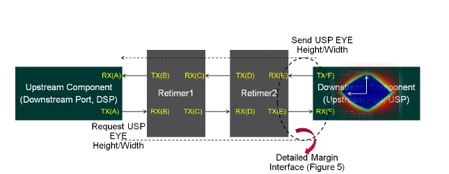
Figure 1: Overview of PCIe Gen4 Lane Margin scheme
Control of lane margining takes the form of commands that direct the receiver to move the sampling point a specified number of steps in time left or right, or a specified number of steps in voltage up or down. Each receiver reports its capabilities in response to software queries. These capabilities include maximum voltage offset, maximum timing offset, number of voltage steps, number of timing steps, timing sampling rate, voltage sampling rate, maximum lanes (maximum number of lanes that can be margined at the same time), independent error sampler, actual data samplers (indicates if margining will produce errors in the data stream or not), etc. Figure 2 shows the allowed ranges for the maximum timing ofset and the maximum voltage offset.
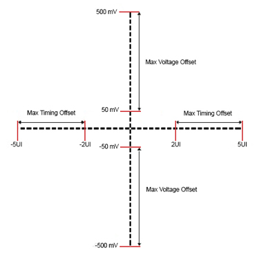
Figure 2: PCIe Two dimensional Gen4 Lane margin in voltage and horizontal direction
The PCIe Gen4 base specification makes allowances for receivers that contain an independent data sampler (in addition to the actual data sampler), or receivers that contain only the actual data sampler. When an independent data sampler is present, errors are detected and reported by the SerDes. In the absence of an independent data sampler, errors are detected in the link by counting the number of detected parity errors and the number of entries in to the LTSSM recovery state. While the specification allows margining in terms of moving the data sample location, the actual margining method is implementation specific. For example, timing/voltage margining can be achieved by injecting an appropriate amount of stress/jitter to the data sample keeping it at its fixed location or by adjusting the data sampler or an independent sampler phase and voltage offset.

Figure 3:PCIe Gen4 l Lane mMargin usage model flow diagram
The full blown margining process for a receiver would include timing margining in both directions and voltage margining in both directions (see Figure 2). It should be noted that support for voltage margining is optional. Figure 3 shows an example of a typical flow diagram for the lane margining process in one direction for timing margining. Each time through the flow, the timing offset is increased. Prior to this process, software will set an error count limit. During the lane margining process, if the error count limit is reached, lane margining is halted, and the receiver is returned to its pre-margining settings. The margin reported by software is the setting previous to the setting that failed.
An example MAC-PHY interface is presented in Figure 4. The PHY does all of the physical measurement of the EYE. The MAC does the protocol level communication encapsulation and de-encapsulation. Usually, the command and status interface between the MAC and PHY is implemented as defined in the Intel PIPE specification [8]. An example decoded command and status interface to the PHY is shown in Figure 4 and is detailed in the PCIe Gen4 specification.

Figure 4: An example device side MAC-PHY signal interface with detailed Logical Sub-Block-SerDes interface
PCIe Gen4 System Stress Sources and Mitigation Strategy
A very simple PCIe system is used to identify the stress sources in a system as shown in Figure 5.
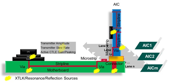
Figure 5: XTLK and coupling in the PCIe section of a system
The dominant sources of system level impairments/coupling/reflection in a PCIe Gen4 system can be identified as [9-11]:
- XTLK sources in a Gen4 system are in device packages, connectors, trace run length and separation, transmitter amplitude, rise/fall time, transmitter de-emphasis, board isolation between transmitter and receiver layers on opposite sides
- Reflection sources in a Gen4 are at cable/trace junctions, via/via stub, connectors, PCB imperfections, roughness, and termination
- Increased insertion loss in PCIe Gen4 reduces the dB differences between Nyquist insertion loss and the base XTLK floor making a PCIe system susceptible to XTLK induced errors.
- Un-Compensable insertion loss deviation due to periodic/a periodic nulls and resonance
- Random noise/pulse width jitter and periodic jitter from various sources in the system
A flexible reconfigurable PCIe system may have 8, 16, 32 etc. lanes or somewhere in between to support high-end graphics to low-end application space. A PCIe controller groups a set of 1xN1, 1xN2 etc. lanes to support multiple simultaneous operating devices. Such bifurcation of lanes into multiple branches of a group of lanes creates interfaces for simultaneous operating devices application space. Each application knows only about its own lanes. Only the host has the global visibility of all lanes and it can initiate any XTLK mitigation scheme using outer layer equalization introduced in this paper.
Due to physical layout of the lanes, from an edge connector to a device end or the host end, some lanes will travel a longer electrical distance than the others. Unless electrical distance is adjusted with wider and thinner traces, the loss seen by one lane will be different from the other lane. The longer lanes will have higher insertion loss compared to the shorter lanes (as shown in Figure 6) making shorter lanes (carrying un-attenuated high energy signal) dominant aggressors compared to longer traces (carrying attenuated weak signal).
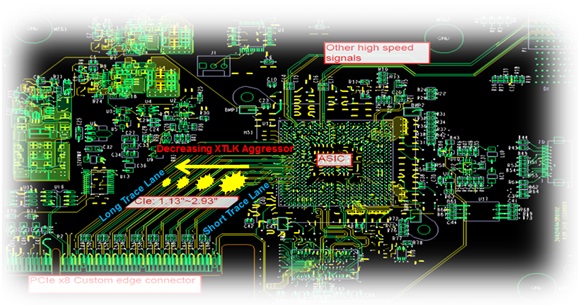
Figure 6: Example XTLK between lanes at dense routing from edge connector to ASIC in an AIC
Usually at a given host/device end, the egress and ingress lanes are on the opposite side of the board to reduce coupling among transmitter and receiver lanes. But the intra lane interaction along the run length in the add-in card (AIC) or motherboard, at the connector or at the package junction is unavoidable. The low-loss lane carrying relatively higher signal swing can be a high impact aggressor to its higher loss neighboring lane that is carrying relatively lower signal swing.
The far end crosstalk (FEXT) from the link partner transmitters to the local receivers travel along the physical traces and continues to couple with other lanes, but its high frequency content attenuates at the same rate as the channel loss along the path. As a result, the FEXT high frequency impact is diminished at the receiver input pin.
On the other hand, the near-end crosstalk (NEXT) from the local transmitter to local receiver behaves differently. In a good design, the transmitters and the receivers are on the opposite sides of the board, resulting in a good isolation and the average XTLK floor is lower. But the spectral energy disparity between low and high frequency content is less. Any significant presence of high frequency NEXT due to poor package isolation between lanes impacts the already attenuated signal spectrum around Nyquist frequency as shown in Figure 7.
There is a need for proper handling of the NEXT spectrum for system-level optimization. The power sum of the NEXT and FEXT is a function of the transmitter launch amplitude, pre/post cursor de-emphasis, and slew rate of the transmitter signal. Adjustment of these transmitter parameters is a good candidate for the proposed outer layer equalization. Based on the slew rate, signal spectrum can be at much higher frequency beyond Nyquist frequency and make a system vulnerable to NEXT (with higher energy floor beyond Nyquist frequency) and to a lesser degree to FEXT (with lower energy floor beyond Nyquist frequency).