Artificial intelligence (AI), together with machine learning (ML), created a huge surge of computing and networking infrastructure needs. This, in turn, has dramatically increased the power consumption of computing and networking chips. Traditional design and validation methods that served us well for decades are no longer able to cope with the new challenges: a paradigm shift is under way of how we design, optimize, and validate our systems and their power distribution network (PDN). In this article, we walk through the evolution of the PDN design and validation process and show what causes this second paradigm shift.
As a child hobbyist, I was introduced to electronics when vacuum-tube radios were still quite common. Small portable radios had already entered the market, with the first ones all using germanium transistors. The simpler units had the so-called “reflex” topology with only two transistors and no bypass capacitor on the supply rail.
Very early computer boards did not need any specific power distribution design. This is illustrated in Figure 1a, which shows a diode-transistor logic card from computing equipment made in the 1970s. It was on a two-sided board, with no ground plane and no bypass capacitor. And many of us remember the prevailing rule of thumb from the 1980s: place a 0.1 uF ceramic capacitor across the power-ground pins of each logic chip, which, back then, usually was a dual-in-line (DIL) package (see Figure 1b).
 Fig. 1 Logic card from an old computer with no bypass capacitor (a), and Apple-1 motherboard with a few ceramic disc bypass capacitors (b).
First
Paradigm Shift
During my career in professional electronics design, the first paradigm shift happened in the mid-to-late 1990s, when the central processing units (CPUs) in computers grew in complexity to the point that they required 10s of amperes of core current. The current transients of CPU core rails required a new approach: power ground plane pairs replaced the power-ground traces, the number and values of bypass capacitors increased, and a systematic frequency-domain design approach was developed. It was based on a calculated impedance target for the power distribution network.1
The impedance target in the 1990s was usually tens or hundreds of milliohms (mΩ), which immediately created a challenge for validation: instrument setups that were to measure impedance were not well suited to measure mΩ on working computer boards. To measure mΩ, the two-port shunt-through measurement setup was developed in 1997, and it has been in use ever since.2
In multi-layer printed circuit boards (PCBs), using one or two plane pairs to serve as the low-impedance supply rails provided low enough series resistance that the horizontal power distribution lumped the entire PDN with tolerably low spatial variations. (As a reminder, the sheet resistance of a one-ounce copper plane is around 0.7 mΩ, which is just a small fraction of a 10 mΩ parallel target impedance.) This was also the time before the widespread use of digital power converters. As a result, such PDNs could be treated as linear and time invariant (LTI) networks, allowing us to use either the time or frequency domain to measure or simulate our circuits, because getting the other domain was straightforward and easy with Fourier transform. An impedance validation example is shown in Figure 2.3 Measuring PDN impedance at the mΩ level was readily doable with the two-port shunt-through scheme by probing the PDN at dedicated power-ground plated through hole pairs with probes connected to the vias from the top and bottom.
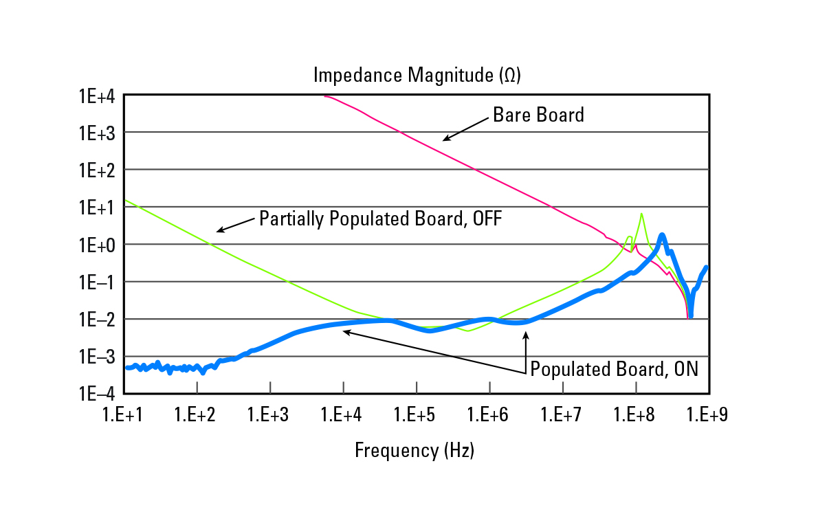
Fig. 2 PDN validation result on a computer board from the mid 2000s.
As the years passed, chips continued to become more power hungry: clock frequencies kept going up, supply voltage continued to drop, and the maximum current draw and current transients were also on the rise. Lower supply voltages require us to set tighter absolute noise budgets, which, when combined with rising current values, resulted in a steeply dropping impedance requirement.
Second Paradigm Shift
The boom of AI and ML accelerated the trend of power-hungry chips, so we have arrived at another paradigm shift. The largest chips now need kiloamperes and require tens of micro-ohms (µΩ) PDN impedance to feed them, creating significant new challenges.
Validating µΩ AC impedance is very complicated with available instrumentation. However, there are even bigger challenges. As illustrated in Figure 3, PDNs cannot be considered lumped any more even at low frequencies, because the series plane impedance becomes comparable to or even bigger than the required parallel PDN impedance. This can result in strong spatial and/or frequency variation of impedance and noise, regardless of whether we look at it in the frequency or in the time domain. In turn, this complicates how we define, design for, and validate PDN requirements.
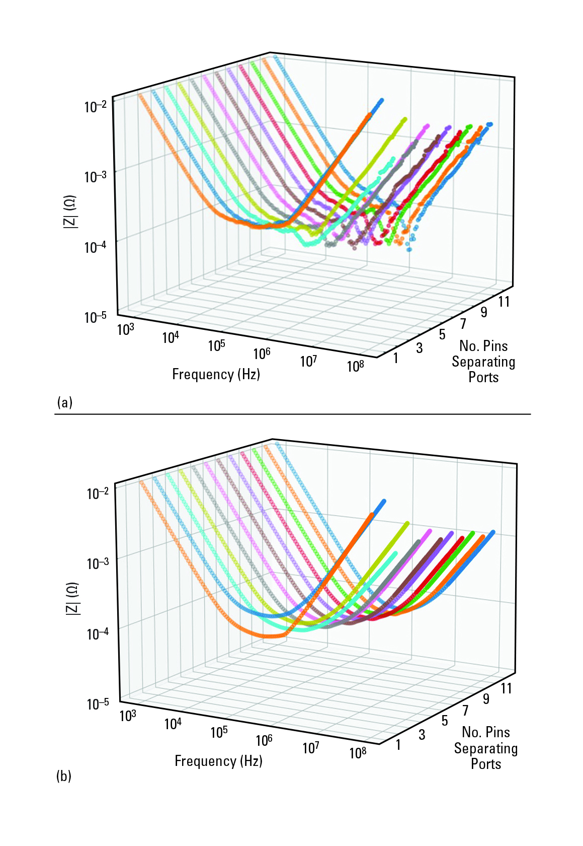
Fig. 3 Measured impedance as a function of pin location under a large computing chip (reproduced from Reference 4).
Very low impedance exposes 3D interactions between probes and the PDN that were previously masked by with higher PDN impedance.5 The 3D rendering in Figure 4a (from Reference 4) shows the probing of the PDN in the footprint of a high current chip. PCBs that make use of blind vias to connect the surface pads to the power planes may lack through-holes, so both probes for the two-port shunt-through testing must be placed on the pads on the same side of the board. Having wafer probes next to each other creates additional inductive loop coupling between the exposed probe tips, which may completely mask out the low DUT impedance we need to measure. Adding to the challenge, this probe tip coupling cannot be calibrated out with today’s vector network analyzer (VNA) calibration methods. 3D rendering of a checker-board via field connecting the chip’s footprint pads to the ground plane (green) and power plane (red) is shown in Figure 4a.
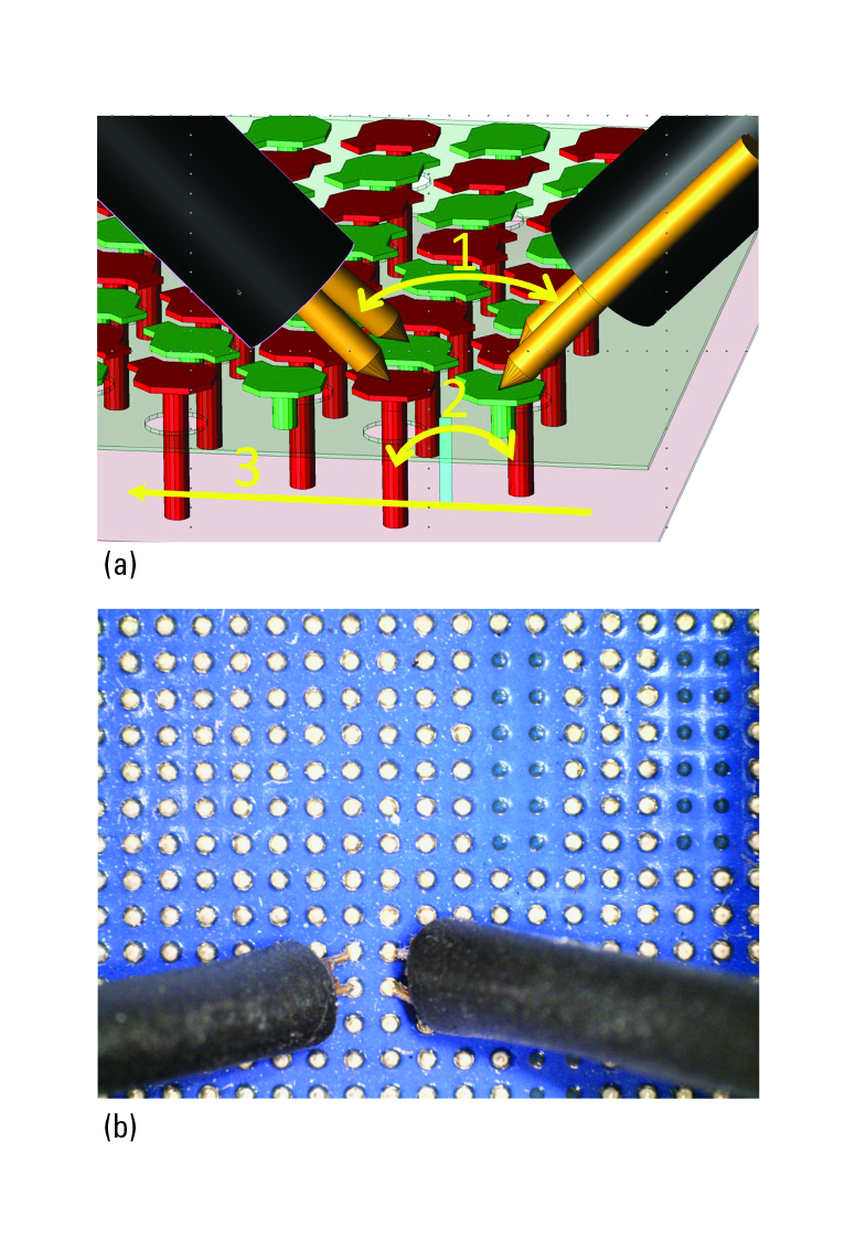
Fig. 4 The three dominant close-field 3D interactions are marked by yellow arrows and numbers: (1) probe-tip coupling, (2) via-barrel coupling, (3) finite plane impedance coupling (a). 1-mm PacketMicro PDN probes landed on a 1-mm via field (b).
As if these challenges were not enough, the component density of our systems and subsystems puts potential noise sources and noise victims closer and closer together, giving rise to increased in-system interference. Figure 5 (reproduced from Reference 6) shows a multi-kW very compact power converter. To reduce distribution loss through the connecting planes, we need to place the power converters close to the chips, where high-speed signals are also concentrated, further increasing the chances for in-system interference.
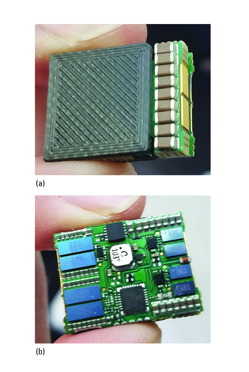
Fig. 5 Vicor high-density power converter circuit top and bottom views (courtesy of Steve Sandler, Picotest).
There are additional challenges as well: the nonlinear functions of digital power converters make PDN validation more complex because the easy conversion between time and frequency domain is valid only in the range of linear operation. The functionality under very large current transients has to be validated differently, such as by a custom fixture, capable of creating large current transients.7
It is still unclear which solutions the industry will settle on to solve these challenges. On the hardware side, an emerging possibility is using a vertical PDN, feeding the high-current supply rails of chips from below the main board while not relying on horizontal power planes in PCBs. However, vertical power distribution requires a significant redesign of the mechanical infrastructure of the system, and it carries its own challenges, including backward compatibility of racks and chassis elements as well as access to test points for validations. In addition, vertical power distribution does not eliminate the spatial variation within the large area required to carry kiloamperes of current. With the spatial variation, the question also remains: Where do we define the test points, and how does that relate to the overall noise specifications?
Evolution of PDN Design
On-chip power distribution design processes have long focused on short-span transient time-domain noise simulations, but one of the earliest systematic off-chip PDN design processes (introduced in the early 1990s) is based on frequency-domain impedance targets. Due to the inherent lowpass filtering of the board-to-silicon path in off-chip PDN designs, the silicon must handle the high end of the power noise spectrum. Because of cost and technological constraints on the chips, lower-frequency bypassing has to be handled in the package and board design. Fortunately, the package and board have successively more space available, but the filtering in the PDN path means we cannot influence the high-frequency noise with components on the user board.
Off-chip impedance-based design and validation approaches focus on linear and time invariant (LTI) systems, and the impedance profile is typically simulated with frequency independent lumped RLC approximation of the off-chip power distribution. Using the frequency domain allows designers to decouple time domain excitation (in most cases highly statistical and able to represent only a few selected working conditions) from the rest of the PDN design and validation workflow.
Off-chip worst-case transient noise estimation, the Reverse Pulse Technique (RPT), was introduced in 2002.8 This process is based on the step response of the PDN. It calculates the absolute worst-case transient noise of a minimal phase LTI system for any arbitrary sequence of current steps with a given transition time. In the early 2000s, the typical design had a combination of clock frequencies in the tens or hundreds of MHz, current consumptions in the 10s of amperes, and one or more 1 oz PCB power-ground planes in the PCB. These system parameters were sufficiently supported with PDN impedances in the tens of mΩ range and allowed designers to largely ignore nonlinearities in the power sources and chips as well as spatial variations on larger server boards.
When current consumption kept rising, DC drop calculations on power ground planes became important and had to be predicted and then validated. As the required DC and AC distribution impedance kept falling, spatial impedance variations became very noticeable. As a result, chip static and dynamic loading effects were added to simulation models. In larger systems, the RC delay caused by the R series plane resistance and the C bulk capacitance could cause enough phase shift between the output of a voltage regulator module (VRM) and its remotely located sense point that it can noticeably reduce the regulator’s phase margin.9
Though the original target impedance approach and the RPT are still valid within the stated boundaries of their applications, applying them to demanding new applications faced multiple challenges: sometimes strong nonlinearities at the power source (voltage clipping), lack of including the silicon and its nonlinearities, and, most importantly, the lack of insight of the inter-relation between the spatially varying PDN transfer functions and spatially varying worst-case transient noise.
Addressing Today’s Challenges
Multiple publications address different aspects of the challenges related to the second paradigm shift. On the system design side, changing from horizontal to vertical power distribution reduces, though does not eliminate, the increasing variability due to the horizontal PDN impedance. Moreover, unless the partitioning and component placement of the bottom-side power source module is optimized for vertical power distribution, the power module may inherit some of the challenges related to horizontal power distribution.
In current design methodologies, optimizing the response of the entire PDN, including the package and chip, offers better overall results.10 However, designers must have access to sufficiently detailed information on all components, including the chip and its package; this is unfortunately not the case for many system and board designers.
Validating very low PDN impedance becomes easier if the test signal power is increased. For example, with two-port VNA measurements, boosting the source power to +20 dBm and using a low noise preamplifier, the equivalent-resistance noise floor of the measurement setup can be reduced to below 1 µΩ.11 Although this addresses the challenge of measuring very low values of PDN impedance, characterizing the spatial variations within big chip footprints still requires a large number of measurements. The limitation stemming from the single-point connection of the VNA measurement setup can be removed by “area illumination,” which has long been available from some of the CPU manufacturers as dedicated test gear. It illuminates the entire footprint (or an arbitrary portion of it) with a large-signal transient source with fast transient capability. Newer implementations are described in References 12 and 13.
While with full-area excitation we can easily measure µΩ impedances, this is restricted to applications where a proper interposer can be made available that matches the exact footprint of the chip and mechanically and thermally fits into the system. Since the large-signal transient exercisers available today can only sink current, they can be used for testing active PDNs only. Moreover, they also do not answer the question about spatial distribution over the illuminated area.
Example PDN Analysis
To illustrate the potentially strong frequency and spatial variation of PDN noise, we take a simplified simulated case from Reference 14. We assume a hypothetical 4 × 4 in. power-ground plane pair with connection/observation nodes on a 1 in. grid. The sketch in Figure 6 shows the geometry, node numbering, and component placement. The frequency and step responses are then simulated with SPICE. Time-domain results are shown in Figure 7.
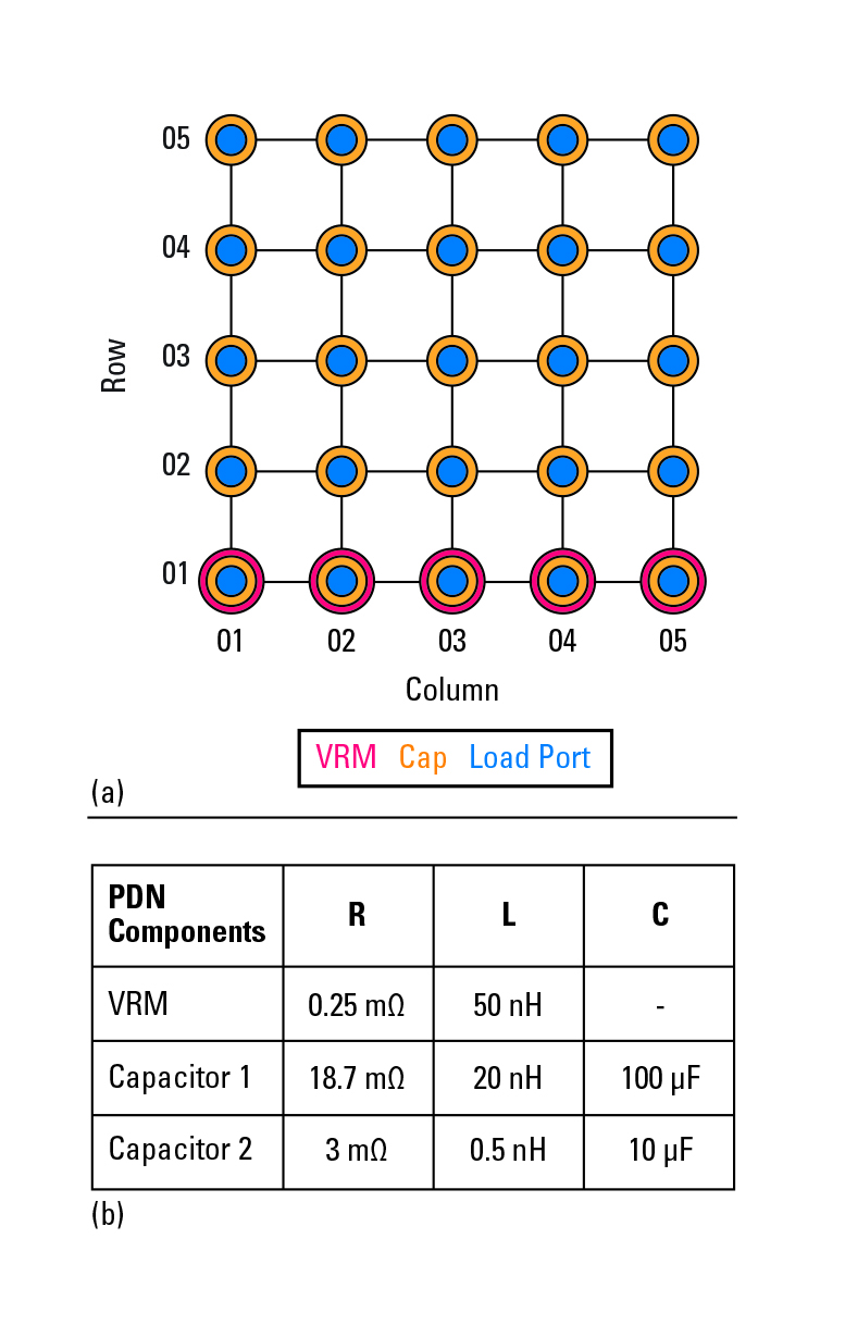
Fig. 6 Node and component placement sketch (a), component values (b).
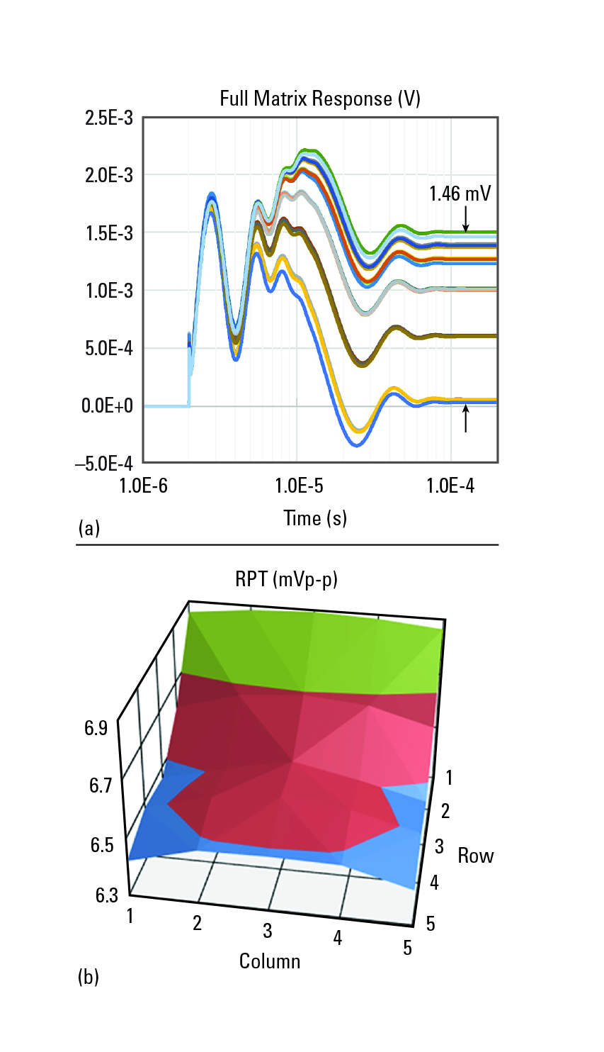
Fig. 7 Frequency-domain response across all 25 nodes (a) and RPT transient-response (b) results simulated on the circuit shown in Figure 6 (b).
In this simple illustration (Figures 6 and 7), circuit values are intentionally exaggerated to clearly show the effect of spatial and frequency variations. Each square inch of the plane pair is represented by a SPICE equivalent circuit with 2.6 mΩ resistance, 142 pH inductance, and 184 pF capacitance. There are two capacitor banks at every node with the cumulative parameters shown in the table. The VRM phases are on the nodes in the first row.
The excitation itself has a uniform distribution of a 1A total value, with equal current sharing and zero skew from node to node. The transient source is a piece-wise-linear step waveform, shaped by a fifth-order Butterworth filter to control the excitation bandwidth, which is set to a 100 MHz cut-off frequency. As explained in Reference 14, when we do AC simulations, the frequency response plot is called AC noise with voltage unit. Even though the total excitation current is 1 A, we don’t call this impedance because the current is distributed across all nodes. The transient noise is calculated with the RPT which is, strictly speaking, applicable to single-node lumped PDNs. For this reason, we don’t call this worst-case noise; we just calculate the peak-to-peak noise with the RPT process.
Summary
With the rapid drop of PDN impedance that is required to feed our biggest chips, design and validation processes have multiple new challenges. The main characteristics of the second paradigm shift is that spatial variance and 3D interactions of close-by PDN features must be considered. These challenges call for new design methodologies and validation processes. End-to-end design flow including VRM and silicon load, vertical power distribution, large-signal transient array loads, and VNA measurements with enhanced accessories are some of the key developments that can help.
Acknowledgement
The author wishes to express his sincere thanks and appreciation to all of his past and current colleagues who shaped his understanding of electronics. A special thanks goes to Janine Love, Samtec, for her expert editing support.
References
- L. Smith, et. al, “Power Distribution System Design Methodology and Capacitor Selection,” IEEE Trans. Adv. Packag., Vol. 22, No. 3, Aug. 1999, pp. 284–291.
- I. Novak, “Why 2-Port Low-Impedance Measurements Still Matter,” Web: http://www.electrical-integrity.com/Quietpower_files/QuietPower-53.pdf.
- I. Novak, “A New Dawn in R&D,” Microwave Magazine, Vol. 12, No. 5, 2011.
- J. Phillips, et al., “Determining the Requirements, Die vs. Package vs. Board: Multi-level Power Distribution Network Design,” DesignCon 2025.
- “3D Connection Artifacts in Modern PDN Measurements,” CadenceLive Boston, September 12, 2023.
- I. Novak, “The Future of Power Integrity through the Eyes of Experience,” Design Con 2023, Web: http://www.electrical-integrity.com/Paper_download_ files/DC23_ TheFutureOfPowerIntegrity_final.pdf.
- S. Sandler, et al., “Design, Simulation, and Validation Challenges of a Scalable 2000 Amp Core Power Rail,” DesignCon 2024.
- V. Drabkin, C. Houghton, I. Kantorovich, and M. Tsuk, “Aperiodic Resonant Excitation of Microprocessor Power Distribution Systems and the Reverse Pulse Technique,” IEEE 11th Topical Meeting on Electrical Performance of Electronic Packaging, 2002.
- J. Hartman, et al., “Impact of Regulator Sense-point Location on PDN Response,” DesignCon 2015.
- I. Zamek, “Reducing Chips Respin Rate by Fixing Common Decoupling Methods Flaws,” DesignCon 2025.
- K. Willis, “Removing Communication Barriers Between CAD and Instrumentation Companies with Open Source PCB,” IEEE EMC-SIPI Symposium, 2025.
- E. Koether and I. Novak, “Transient Load Tester for Time Domain PDN Validation,” EDI CON 2017.
- S. Sandler, B. Dannan, H. Barnes, I. Ben Ezara, and Y. Ni, “Design, Simulation, and Validation Challenges of a Scalable 2000 Amp Core Power Rail,” DesignCon 2024.
- E. Koether, et al., “Bridging the Time-Frequency Chasm in PDN Design: Leveraging Cumulative Power-Rail Noise and Reverse Pulse Techniques for Spatial-Frequency Insight,” DesignCon 2026.
