
IBIS-AMI models have been around for a decade and evolved to provide off-chip and system designers an efficient way to assess link performance of high-speed electrical interfaces with transceivers implementing various combination of equalization techniques. As with any model, for IBIS-AMI to be useful they need to be benchmarked and carefully correlated to real-world silicon performance of the transmitter and receiver they represent. With the advent of multi-standard DSP IPs, modern transceivers can operate over a wide range of operating points on the electrical interface spectrum. Although the underlying architecture of the IP remains the same for different protocols, corresponding to the same IBIS-AMI models, some care needs to be applied when it comes to the correlation and tuning of the underlying behavioral models against silicon performance, as different operating points (such as the electrical interface, channel loss range, and baud rate) dictate different sets of constraints and measurable quantities that are available in a lab environment. The capability to match simulation and real-world performance across not only one operating point, but multiple, makes modeling each instantiation that much harder, yet that much more necessary to ensure proper operation in these increasingly challenging links. In this paper, we demonstrate a step-by-step correlation methodology adapted for DSP-based PCIe Gen5 and Gen6 IBIS-AMI models where we can measure and directly correlate raw errors out of the DSP on a test setup that is based on the receiver stress eye methodology of the PCIe standard.
The receiver IBIS-AMI model used for correlation is built upon our previous work. The block diagram showing the signal data path through the behavioral equalizer blocks included in the algorithmic representation of the PCIe IP. The model includes two types of intrinsic noise impairments that will be used to tune its performance. A receiver’s input referred noise, which is amplified by the CTLE, will have a larger effect on longer channels which require more CTLE gain. Another source of noise will be injected as uniform random noise after the ADC stage.
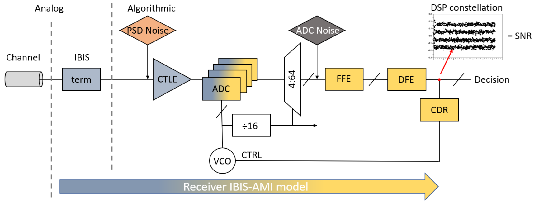 Figure 1. DSP Receiver IBIS-AMI Block Diagram.
The two noise sources embedded in the behavioral model are put in place to tune minor mismatches between the actual block response of the IP that is being modeled and the behavioral version implemented in the algorithmic model. These two knobs are essential in achieving good correlation and providing a versatile model that can be tuned to bound the IP performance as seen in the real silicon at 112 Gb/s, and this paper focused on extending the coverage to 32 Gb/s and 64 Gb/s to match lab performance.
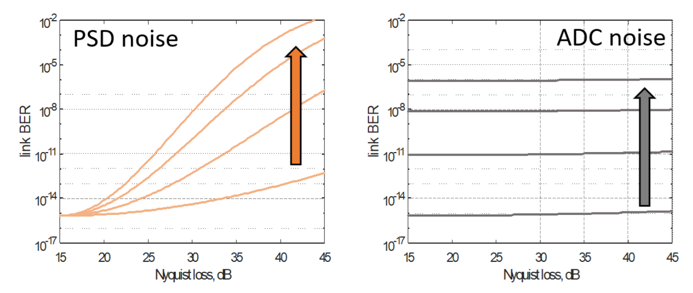 Figure 2. IBIS-AMI link BER sensitivity to noise sources.
The SNR of the equalized DSP sample constellations is chosen as the figure of merit to link lab performance measurement to simulation prediction because it can be computed with the baud rate sampled constellation only, can be calculated with a computationally reasonable amount of symbols, and has an analytical relationship to the link BER for a given modulation. This relationship allows us to correlate model predicted performance to the raw symbol errors recorded after the receiver equalization in the lab.
The PCIe standard provides a fair mechanism to test PCIe receiver impartially by using a carefully stressed electrical signal to drive the device under test. Our methodology includes a calibrated reference equalizer, so the performance of the link under a 100 MHz single tone sinusoidal jitter stressed signal as described in “PCI Express® Base Specification Revision 6.0.1 Version 1.0 - 8.4.2 Stressed Eye Test” is compared and correlated to the simulation. The model receiver’s intrinsic impairments are adjusted to achieve a reasonable correlation in term of the performance for this injected stressed signal. The process, repeated over variances of the IP, including parts, supply, and temperature provides a correlation model that bounds the performance as observed on the test chip. Given the baud rate CDR architecture that is present in the IP and implemented in the IBIS-AMI model, the injected single 100 MHz tone will directly translate to non-ideal sampling location and yield a DSP constellation with a degraded SNR. This choice is reinforced due to the nature of the algorithmic model and its main use as a prediction tool for high-frequency signal integrity issue arising from interconnect design.
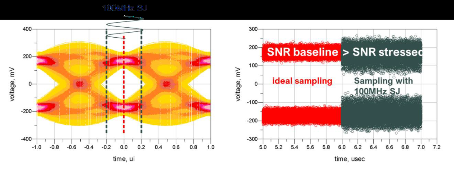 Figure 3. 100MHz single tone jitter sampling and SNR degradation.
Before being able to correlate with silicon, this new approach requires an additional calibration step that needs to be performed and aligned in both the lab and simulation environment to ensure the calibrated stressed signal will provide a measurable BER in the lab and that the simulation model is being driven by the same stress condition. The calibration itself relies on the definition of a minimum receiver architecture being able to equalize such a signal. The reference receiver implements behavioral signal conditioning equalizer that will be described in subsequent sections as they will need to be implemented within the simulation framework as well. Further details on our lab calibration setup, our simulation calibration setup, the implementation of calibration and testing regression at 32 Gb/s and 64 Gb/s in the lab and in simulation can be found in the complete paper.
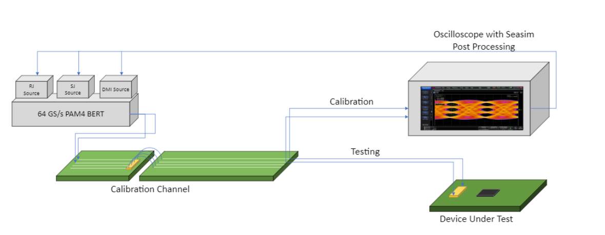 Figure 4. Stress calibration setup for 32.0 GT/s and 64.0 GT/s from PCI Express® Base Specification Revision 6.0.1 Version 1.0.
Our previous DSP behavioral model correlation methodology fell short of being able to gather quantitative BER data for PCIe IBIS-AMI model comparisons, due to the specific challenges of the technology. A methodology of a device loopback over channel insertion losses as used in the previous 112G correlation work would not provide enough raw errors to be able to draw trends and tune the model against the hardware. Extrapolation was discarded as it would be difficult to implement properly and would not scale for correlation with real product if needs be. A methodology amendment keeping the current IBIS-AMI modeling process and figure of merit calculation the same while adjusting the channel and stressed input signal characteristics was proposed based on the stress calibration methodology similar to the PCIe standard. The DUT direct error measurement flow was conserved. A unified setup and procedure were achieved for the lab and simulation instances using reference equalizer models and post-processing. A device implementing a PCIe receiver operating at 32 GT/s IBIS-AMI model could then be regressed over their tuning knobs to achieve alignment against the jitter tolerance achieve in the lab. The concept of a general reference receiver and transmitter is not novel in standards such as PCIe and Ethernet, but creating reference receivers and transmitters that reflect real products enables greater confidence in tape-outs, where first time success is critical to keeping pace with the interconnect demands of the present and future.
The paper referenced here received the Best Paper Award at DesignCon 2023. To read the entire DesignCon 2023 paper, download the PDF.