
Peripheral component interconnect express (PCIe) is an interface standard for connecting high speed components in modern personal computers. The common electrical interface (CEI) plug-in card specification has a tight thickness limit of 0.062 in. driven by the connector on the host mother board. Because of the thickness restrictions, the PCB stackups are limited to the number of layers that can be used. Often power (PWR) layers are used for signal reference planes.
To exacerbate the problem, many silicon vendor application notes advocate partitioning VDDQ power layers for double data rate (DDR) command/address (CA) memory signals. Frequently power or even ground (GND) layers are partitioned to fulfill these guidelines, and, if not careful, these or other signals referencing these layers may inadvertently cross over the split.
It is well known that crossing a split plane will excite slot-mode resonance in microstrip layers leading to crosstalk and other EMI issues. In fact I wrote a Signal Integrity Journal (SIJ) article on this subject back in 2018 [1]. But what about when stripline traces cross one of the split reference planes?
There is often a debate in the SI community claiming for stripline, it is ok to cross a split power plane, so long as the other adjacent reference plane is solid; implying that the solid reference plane will return the current. Or others claim if there is an adjacent solid reference plane, less than 5mils away under the split, crosstalk will be mitigated.
To investigate this I asked my friend and fellow SIJ Editorial Advisory Board (EAB) member, Yuriy Shlepnev from Simberian Inc. to set up several test cases and do some simulations for me using his company’s Simbeor THz electromagnetic (EM) software [2]. Here is the analysis.
Test Models and Simulation Case Studies
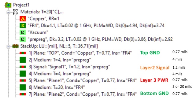
The generic stackup is shown in Figure 1. The top layer is the GND reference plane. Layer 2 is the signal layer. Layer 3 is the PWR reference plane. The bottom is a GND reference plane.
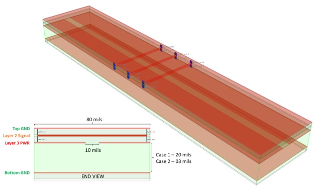
For future comparison, a baseline simulation (Case 0) was set up with three traces routed between two solid reference planes (Top GND and Layer 3 PWR) as shown in Figure 2. Bottom GND layer was not needed, so it wasn’t included in the simulation. Trace widths were 4 mils wide, 400 mils long with 28 mil center-center separation. Impedance was ~50 Ohms single-ended. The center trace is the aggressor with two victim traces on either side.
Figure 2 shows peak surface current density at 40 GHz on the solid PWR and GND reference planes. As can be seen, the return current flows in the opposite direction, parallel to the center trace current. The 28-mil trace separation ensures little or no return current flows under the victim traces.

The physical cross-section of the substrate showing three traces crossing a 10-mil wide slot is shown in Figure 3. Case 1 simulations used a 20-mil thick PWR/GND cavity between plane layers 5 and 7, while Case 2 simulations had a 3-mil cavity.
Three EM power flow density simulations were performed at 10 GHz, 20GHz, and 40GHz for each case study. Figure 4 shows the results for Case 0 (top row), Case 1 (middle row) and Case 2 (bottom row). Absorbing boundary conditions were used in all simulations.
For Case 0, we observe power flow density is well guided by the transmission line structure and follows the center trace. There is no coupling to victim traces. But for Case 1 and Case 2 we see parallel plane waves launched into the plane cavities as the signal crosses the split. It is analogous to a pebble being dropped into a pool of water. With 20 mil dielectric below the split plane, we observe there is more energy coupled to victim traces.

Figure 5 is more interesting. It compares the peak surface current density on three planes. The bottom GND plane is shown on the left. Layer 3 PWR split plane shown in the center, and top GND reference plane shown on the right. Frequency was 40 GHz.
As the signal changes polarity while crossing the split plane, we observe return current diverted in opposite directions along the edge of the split. This excites slot-mode resonance and launches a parallel plane wave through the plane cavities as shown in Figure 4 power flow simulation results above. This in turn generates eddy currents on the reference planes.
On the top GND reference plane, shown in Figure 5, we observe the return current has a circular rotation pattern with opposite direction; each side of the center trace. This coincides with the opposite direction of current along the slot edge of the adjacent plane. These eddy currents couple noise onto the victim traces.
With respect to the center split PWR planes in Figure 5, we can clearly see the current traveling along the slot edge and current flowing along the victim traces. There is no difference in current density on the split plane between Case 1 and Case 2. This is to be expected because the PWR/GND cavities between top layer and layer 3 are the same thickness for both.
But on the bottom GND plane below the split plane, shown on the left in Figure 5, we can see there is higher current density equivalent to the center trace position as it crosses the split for Case 2. This is predictable since it has closer proximity to the split plane and trace above it than Case 1.
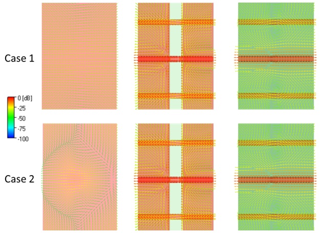
Figure 6 summarizes and compares the surface current density of solid PWR/GND reference planes vs. a split PWR and solid GND reference planes. The return current on the solid reference planes are concentrated mainly under the center trace. The return currents on the split PWR/GND planes circulate over the surface due to slot-mode resonance caused by current flowing along the edges of the split planes. The circulating currents under the victim traces couple the crosstalk noise onto the victim traces in spite of having 28 mils separation from aggressor trace.
The other interesting observation on the top GND reference planes shown on the right in Figure 6. Contrary to some popular belief I mentioned earlier, current density does not increase on the adjacent reference plane to compensate for the discontinuity of the split reference plane.

In this section we can conclude:
- With two solid reference planes, return current flows in the opposite direction and parallel to the trace current. A trace separation much greater than 3x line width ensures little or no return current flows under the victim traces.
- In stripline geometry, traces have return current on both reference planes and behave much like microstrip traces crossing a split plane.
- A thicker plane cavity under a split plane results in more energy coupled into the cavity below the split, resulting in more energy coupled onto the victim traces in spite of the wide separation of victim traces.
- In stripline geometry, current density doesn’t increase on the other solid reference plane adjacent to the trace to compensate for the discontinuity of the split reference plane.
Crosstalk Analysis
An interconnect bandwidth (BW) with knee frequency (f_knee) up to the 5th harmonic of the fundamental frequency preserves the integrity of risetimes (RT) down to 7% of the period of the fundamental frequency.
If
RT*BW = 0.35
then
RT = 0.35/f_knee
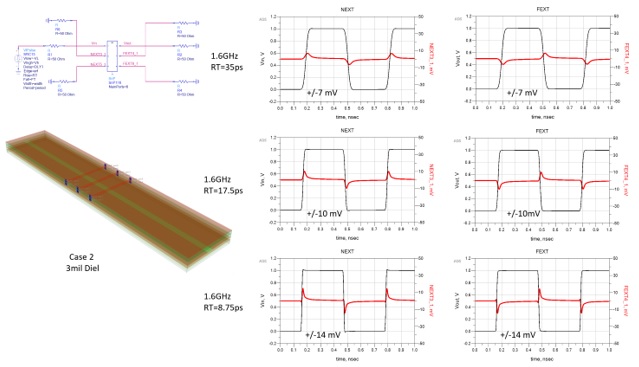
Given 10 GHz, 20 GHz, and 40 GHz are knee frequencies, the respective risetimes were calculated and used for transient simulation using Keysight ADS [3] software. A 1.6 GHz clock was used as an aggressor to the center conductor. Near-end and far-end crosstalk (NEXT/FEXT) for Case1 and 2 were simulated. The results are plotted in Figure 7 and Figure 8 respectively. Since all three traces had the same spacing between them, crosstalk is the same for each victim, so only a single adjacent trace crosstalk is shown for clarity.
In both cases, NEXT/FEXT increased as the RT decreased. When the dielectric thickness was reduced from 20 mils to 3 mils under the split, crosstalk was reduced by 46% for 35ps RT, 58% for 17.5 ps RT and 64% for 8.75 ps RT.
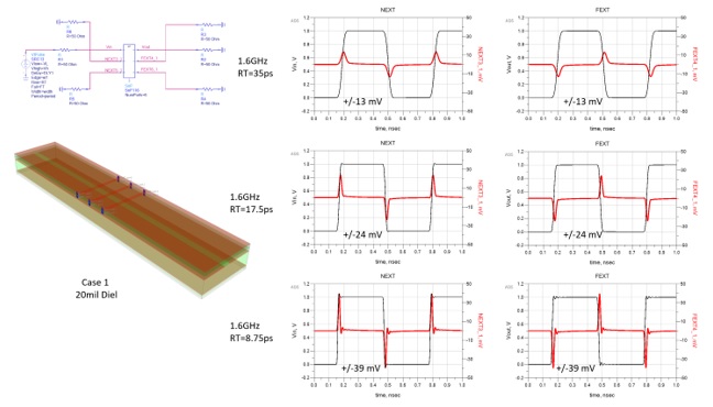
Figure 7. Keysight ADS transient simulation results for Case 1 geometry showing NEXT/FEXT (red) for RT= 35 ps (f_knee 10 GHz), RT= 17.5 ps (f_knee 20 GHz) and RT= 8.75 ps (f_knee 40 GHz).
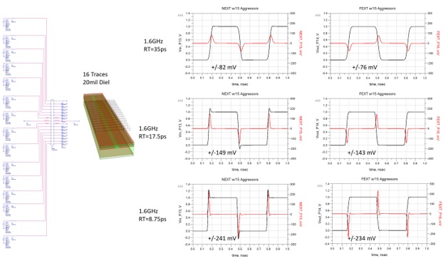
The EM simulations were repeated, this time using a model with 16 traces crossing the split. With 15 aggressors and single victim in the middle of the bus, the results are shown in Figure 9 and Figure 10. With all 15 aggressors switching simultaneously, NEXT and FEXT dramatically increased ~ 6-7 times for each case.

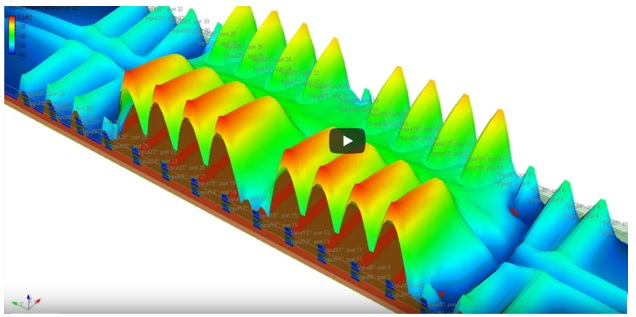
To check out more about crosstalk when multiple stripline traces cross a split plane, check out this cool video from Yuriy Shlepnev, “How Interconnects Work: Crosstalk in Multiple Striplines Over Split Planes With Close Solid Plane” [5].
Summary and Conclusions
At the start of this article, I mentioned there is often a debate claiming it is ok to cross a split power plane, as long as the other reference plane has a solid reference plane, implying that the solid reference plane will return the current to compensate for the discontinuity of the split plane. Contrary to this popular belief, current density does not increase on the other solid reference plane. In fact, we have seen that stripline traces have return current on both reference planes and behave much like microstrip traces crossing a split plane.
We have also verified that as long as there is an adjacent solid reference plane under the split, vertically separated by less than 5 mils, crosstalk is significantly reduced, but not eliminated. As Figure 12 summarizes, the amount of crosstalk is a function of how many aggressors signals also cross the split and risetime. The faster the risetime, the higher the crosstalk. The greater the distance to the next reference plane, the higher the crosstalk.

But we also acknowledge risetime degrades due to dispersion because of losses due to dielectric. This means depending on the distance of the split relative the signal launch point, crosstalk may not be as much of an issue. It depends on your system noise budget.
In conclusion, stripline geometry still has return currents flowing on both reference planes. The proximity of the trace to each plane determines how much current flows on each reference plane. More return current flows on the plane closest to the trace. Because there is a split on one of the reference planes, there will still be current flowing along the slot. If the split reference plane is at the top or bottom of the stackup, then there is still risk of EMI and failing EMC testing.
When you cannot avoid a split plane, a more detailed analysis should be done based on the actual layout, stackup of the board, and properties of the signals crossing the split.
References
- Bert Simonovich, “Split Planes and What Happens When Microstrip Signals Cross Them,” Signal Integrity Journal, January 16, 2018
- Simbeor THz [computer software], (Version 2020), https://www.simberian.com/
- Keysight Advanced Design System (ADS) [computer software], (Version 2016: http://www.keysight.com/en/pc-1297113/advanced-design-system-ads?nid=-34346.0&cc=CA&lc=eng
- PCI Express® External Cabling Specification, Revision 1.0, January 4, 2007
- Yuriy Shlepnev, “How Interconnects Work: Crosstalk in Multiple Striplines Over Split Planes With Close Solid Plane”, https://youtu.be/p6Y-JhLG3wA