
Semiconductor signal conditioning and signal recovery innovations have extended data rates by managing allowable signal-to-noise ratio (SNR) at progressively higher Nyquist frequencies. We have experienced how each successive signaling technology increases the electro-mechanical design resolution needed to address the channel physics while respecting the SNR of the chips. These movements throughout the years have provided a baseline of traditional design goals that lead us to better understand today’s 224 Gbps-PAM4 (Pulse Amplitude Modulation) physical layer requirements.
Historical Evolution
As we move through the speed grades, the physical layer design of printed circuit boards (PCBs), cables assemblies, and connectors evolves. The latest data throughput and latency-driven signaling updates challenge previously acceptable design trade-offs.
The requirements for high-speed data transmission continue to increase to meet market demands, including cloud computing, artificial intelligence, 5G, and the Internet of Things. Although there are overlaps in the details, a brief overview of how we got to where we are today will help illustrate the technological progression from 1 Gbps transmission line data rates to the 224 Gbps rates of today.
Approximately 30 years ago, the discussion centered around return to zero (RZ) versus non-return to zero (NRZ). Most signaling inside the data center (within or between boxes) was single-ended until twisted-pair Ethernet came along.
Let’s not forget about those adventurous engineers at Cray, who pushed the envelope to support NASA workloads running across multiple compute nodes at 80 MHz data rates using differential pairs. In comparison, the first IBM PCs around the same time were clocked under 4.77 MHz.
This is when processor clocks were divided instead of multiplied. PCBs moved from wiring boards to multilayer FR4 and were literally “taped-out” by hand using actual tape; multiwire cables were used for printers and coax for networks; RJ-45 was used for telephones; and integrated circuits replaced individual components on printed wiring boards. In the lab, it was still possible to prototype circuits using protoboards and measure signals with an oscilloscope. For simulation, lumped values (L, R, C, k) were sufficient to model most discontinuities.
Roughly 20 years ago, NRZ signaling started to dominate the mental model. Moving from 1 Gbps-NRZ to 3 Gbps-NRZ and then 6 Gbps-NRZ, each data rate step increased mechanical/electrical design attention on geometrical changes, but generally still treated the connector or PCB as a lumped loss component.
The introduction of NRZ design requirements effectively doubled the channel bandwidth while being more susceptible to noise. To reduce data errors, SNR was improved by increasing power and adding equalization techniques.
Electronic design automation (EDA) for PCBs started to arrive along with Gerber files. Connector technology for data included the edge card and 9-pin d-sub. Scope probe loading neared its limit, vector network analyzers (VNAs) became commonplace, and fast Fourier transform (FFT) analysis became prevalent. For simulation, lumped values (L, R, C, k) were sometimes in place, while behavioral SPICE models were incorporated in transmission line simulations to simulate discontinuities.
About 15 years ago, the transition started moving from 10 Gbps-NRZ to 16 Gbps-NRZ and then 25 Gbps-NRZ. Backplane cables emerged as the norm, with many companies creating backplane demonstration boards to mimic applications with 1 m trace lengths.
As a result, lumped component models for connectors or transmission line discontinuities were no longer sufficient. Although common in the RF industry, everyday bond wires, PCB vias, and connector segments were represented with their own S-parameter components. Crosstalk evolved as an increasingly critical consideration in the design space.
Signal integrity labs had 50/100 Ω data generators with high-bandwidth sampling oscilloscopes for time domain analysis. Next to every time domain test system was a VNA. Sometimes high frequency probe stations were used, but most of the test fixturing was based on SMA launches. Around this time, a specialized group of signal integrity practitioners emerged from the electrical engineering ranks.
Just around 10 years ago, the march from 28 Gbps-NRZ to 56 Gbps-PAM4 began affecting transmission line design while representing an important signaling change in modulation from NRZ to PAM4. With the goal to further increase data rates, the industry adopted PAM from the optical industry. “PAM4” is ubiquitous in the optical domain, which made it easier to adopt into long-reach copper interconnects compared to other modulation schemes.
In copper, PAM4 uses four voltage levels to represent two-bits of data per symbol. By encoding two or more bits per symbol, PAM increases the data rate without increasing the required channel bandwidth. The consequences to signaling and transmission line design include greater sensitivity to noise and insertion loss deviation.
This generally transitioned the industry from 28 Gbps-NRZ to 56 Gbps-PAM4, or in the case of PCIe, from 32 Gbps-NRZ to 64 Gbps-PAM4. The application space was either networking or computing. In both cases, the channel design respected the same unit interval (UI) and Nyquist frequency. The downside was resulting multiple signaling levels required a better channel SNR, forcing specific attention to unintentionally couple signals (crosstalk) and insertion loss.
This step placed greater emphasis on crosstalk, especially near-end and on transitions between components: connectors-to-PCBs, connectors-to-cables PCBs, and connectors-to-connectors. Test equipment in the lab was primarily VNAs. Reducing stubs in PCBs (back-drilling) and connectors was the new mission.
The correlation between measured S-parameters and predictive analysis for high frequency simulators became critical to ensuring that time domain simulations could properly estimate bit error rate (BER). With Ethernet for cloud computing and IoT, the line data rate went from 56 Gbps-PAM4 to 112 Gbps-PAM4, doubling the Nyquist frequency to approximately 28 GHz to support the 112G-PAM4.
Design attention focused on impedance transitions along shorter connector paths and electrical stubs ~1 mm and longer. At the same time, channels went from 16 lanes to 32 lanes, doubling the effective throughputs in the same amount of front panel space.
Density increases were directionally opposite to design methods that separated lines to reduce noise. Instead, transmitter and receiver pair groupings are commonly used to reduce near-end coupling impact. Selective channel grouping in PCB uses different layers for transmit and receive to reduce noise. Connector designs purposely put larger physical gaps between transmit and receive pairs.
Electrical labs and production lines use 67 GHz VNAs. Engineers typically do time domain analysis with production silicon. As a result, signal integrity engineering has emerged as its own discipline.
Emerging Technology
The transition from 112 Gbps-PAM4 to 224 Gpbs-PAM4 doubles the Nyquist frequency. Previously, speed transitions took three to five years. Now, we see 224 Gbps-PAM designs happening before 112 Gbps-PAM4 has even had the chance to become a volume leader.
Signal integrity engineers now are worried about stubs, transmission line discontinuities, and apertures of ~0.7 mm. This means we are now sub-mm in our design space. To put this in perspective, the entire channel can be over 1 m in length, with each discontinuity interdependent on physical transitions both before and after the immediate area of concern.
Wavelengths are now small enough that typical apertures (resonance cavities) are as important as the signal path. Apertures, whether in the signal, return path, or between components, have become a critical part of transmission line design.
224 Gbps-PAM4 Design Challenges
For a clearer understanding of how 224G-PAM4 targets impact design, let’s consider basic signal integrity challenges of correlation, transmission-line imbalance, and within pair skew.
Model-to-Measurement Correlations
Meeting time-to-design (a step earlier than time-to-market) requires advanced predictive analytical techniques and methods. It is not always possible to build and tune the physical channel times before engineering silicon arrives, which means the models need to be as accurate as possible. In addition, any deviations between modeled and predicted correlations must be understood to meet time-to-design goals.
In the frequency domain, removing errors from test boards is critical. The improvement cycle includes test equipment, test fixturing, calibration (fixture removal), and test boards. With these systems often costing close to $1M, it is also worth considering what is absolutely required in the production environment.
It’s increasingly critical to have design correlation between measurements and models. Any errors that are in the frequency domain can show up in the time domain. For “measurement to model” correlations, the following scenarios should be considered:
- If measurement is worse than modeled, how do you respond?
- If measurement is better than modeled, what do you believe?
- What is a good correlation? Within 1dB?
- If yes, for which frequency parameters?
- How does each frequency domain parameters impact eye closure?
- How does each frequency domain parameters impact BER?
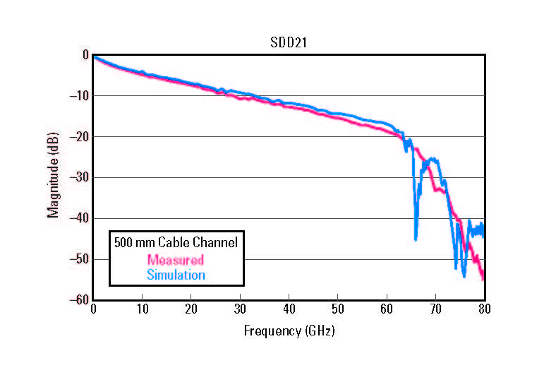 Figure 1. Insertion loss plot of a two-connector channel example consisting of a connector and 500 mm cable assembly.
Unfortunately, when in predictive mode, we do not know the actual results. If the insertion loss is within budget, should we be pleased with this alignment? If only considering the predictive results, time would be spent removing the resonance spike when it may have been more effective to focus on lower frequency losses.
Early measurements improve focus. In this example, knowing there is a difference between the simulation resonance spike and the measurement’s smooth roll-off helps us understand the actual channel, and therefore improve the time-to-design. The difference in the insertion loss will aid in directing a better understanding of the physics associated with broadband response.
Transmission Line Imbalance
Let’s consider the same 500 mm channel from the example above. But this time, let’s intentionally add a perturbation (see Figure 2). In the real world, this could represent a mismatched solder volume between the P and N wires.
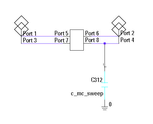 Figure 2. Model of a two-connector channel example consisting of a connector and 500 mm cable assembly with an intentionally added perturbation.
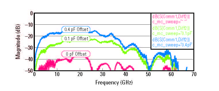 Figure 3. Insertion loss plot two-connector channel example with intentionally added perturbation. From bottom to top: Ideal balanced channel to others with increased capacitive offsets.
 Figure 4. Eye diagrams generated from pseudorandom binary sequence bitstreams for tow-connector channel example. From left to right: Ideal balanced channel to others with increased capacitive offsets.
Within Pair Skew
During the design process, there is much time and energy spent on eliminating skew from transmission lines. Skew is certainly important for reasons others in the industry have highlighted.
The channel in the example below is pad-to-pad as before, but in this instance, it has two cable assemblies interconnected for a total length of over 1 m. This is a three-connector channel example consisting of a connector, 200 mm cable assembly, connector, 500 mm cable assembly, and another connector.
For this study, there is a lossless delay artificially added on one of the lines that could be a PCB skew impairment as shown in Figure 5. The three-connectors are contained in the center S-parameter block.
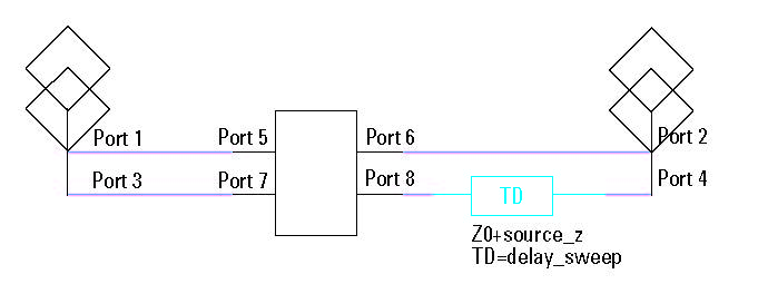 Figure 5. Model of a three-connector channel example consisting of a connector, 200 mm cable assembly, connector, 500 mm cable assembly, and another connector with a lossless delay added.
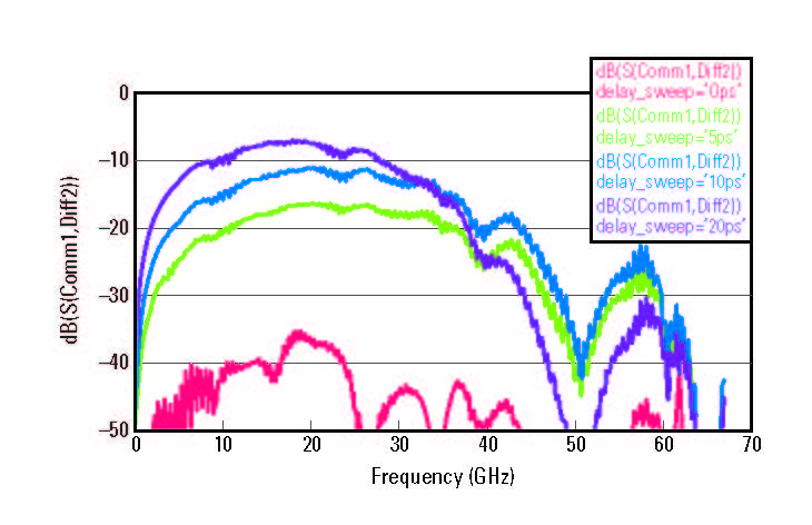 Figure 6. Insertion loss plot of a three-connector channel example with a lossless delay added. From bottom to top: 0 to 20 ps of artificially introduced skew.
The eye diagrams in Figure 7 shows that moving from the ideal channel to one with a different amount of skew impacts the eye diagram. From the data integrity perspective, even at 5 ps of delay, there is an appreciable reduction in eye opening, resulting in a lower channel margin.
In summary, time domain eye closure and frequency domain mode conversion can have similar responses caused by different aberrations. Be sure to look at minor design and process variations when evaluating how frequency domain lab results are represented in time domain.
 Figure 7. Eye diagrams generated from pseudorandom binary sequence bitstreams for three-connector channel example. From left to right: 0 to 20 ps of artificially introduced skew.
Design Considerations for 224 Gbps-PAM4
- A cross-functional design approach is best: System architects working in collaboration with cable/connector and semiconductor teams to support an application is the fastest way to a channel. Teams need to engage early in the channel development process to deliver extensible and scalable architectures. Important roles and areas of concern include hardware engineering, system architects, signal integrity, mechanical integrity, and thermal.
- Define performance targets first, specifications second: Start with targets giving contributors a chance to co-develop operational budgets that can later be broken down into components. Be transparent with margins. Specifications then come from operational prototype and correlated models.
- Confirm with correlation: Make sure there are model-to-measurement correlations for both S-parameters and time domain. Understand how frequency domain parameters relate to the time domain results.
- Applications need both signal integrity and mechanical integrity: Even as the signal requirements become more critical, the signal density requirements (differential pairs per square) continue to increase between generations. This means greater design effort is needed for mechanical parameters such as normal forces, mechanical robustness, and wipe. All of these intertwine with the application form factor (server chassis and cooling). Small deviations from intended design can reduce channel margin.
Conclusion
Application needs have driven data transfer speeds from 1 Gbps-NRZ to 224 Gbps-PAM4. Each step forward requires a better understanding of transmission line design, material physics, and system architecture options to scale to the highest density, mechanically robust physical layer. There is still engineering to do in 224 Gbps line rates; fortunately, today’s tools and methods are better than ever and continually improving. Looking ahead, it will be interesting to see what the next 30 years will bring.