
This article is part two of a two-part series. Please find part one here.
Introduction
In the previous article, we delved into the fundamental architecture of the PCIe Card Electromechanical (CEM) connector, exploring the nuances in Signal Integrity (SI) performance criteria between PCIe Gen6 and Gen7. We focused on both connector-only performance and overall channel performance, emphasizing additional design considerations for Add-In Cards (AIC) and baseboard/motherboard to push the insertion loss drop off frequency, alongside simulation parameters and material choices for the housing of the connector. In this article, we pivot to showcase a marked improvement in SI performance, specifically in connector-only scenarios, by transitioning from a microstrip to a stripline footprint design.
Illustrated in Figure 1, we present a simulated impedance analysis contrasting the PCIe Gen7 CEM connector's performance using both microstrip and stripline footprints. This comparison is meticulously controlled to ensure parity pad lengths on the AIC and baseboard remain consistent across both footprints for a fair comparison. As is evident from the impedance comparison of this connector only performance of this CEM connector, it encompasses AIC footprint from 1.0 ns to 1.05 ns, the electrical length of the connector between 1.05 ns and 1.11 ns, and the baseboard footprint from 1.11 ns to 1.16 ns.
The frequency masks employed for insertion loss (IL), return loss (RL), and crosstalk assessments are augmented versions of the Gen6 standards, which traditionally cap at 24 GHz. For the Gen7 connector analysis, these have been extended to 40 GHz to accommodate the higher Nyquist frequency of the Gen7 connector. The stripline footprint demonstrates superior signal integrity performance, as evidenced by the IL and RL plots in Figure 2 and Figure 3, at frequencies beyond 24 GHz.
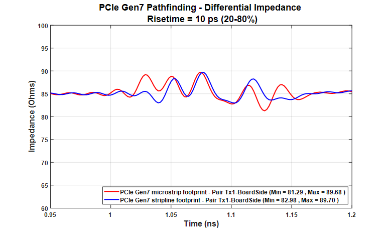 Figure 1. Impedance comparison of Gen7 connector, microstrip vs. stripline footprint.
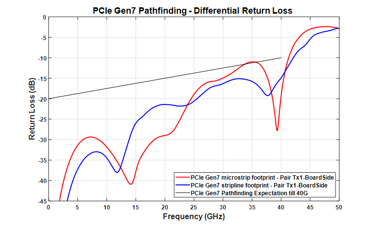 Figure 2. Return loss comparison of Gen7 connector, microstrip vs. stripline footprint.
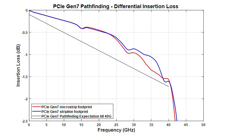 Figure 3. Insertion loss comparison of Gen7 Connector, microstrip vs. stripline footprint.
When comparing the Near-End Crosstalk (NEXT) and Far-End Crosstalk (FEXT) between the two models, it was observed that the NEXT values are remarkably similar, rendering their presentation here unnecessary. In the comparison of FEXT, it is evident that the baseline crosstalk performance of the stripline footprint outperforms that of the microstrip footprint. To quantify this performance difference, the Component Contribution Integrated Crosstalk Noise (CCICN) calculation was employed. This analysis revealed that the CCICN FEXT value for the stripline footprint is 125 uV, while for the microstrip footprint, it stands at 140 uV, further illustrating the superior crosstalk characteristics of the stripline configuration.
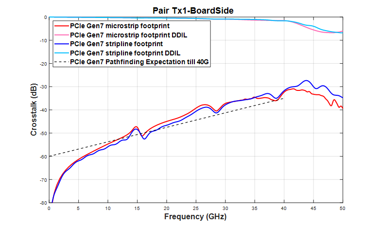 Figure 4. FEXT comparison of Gen7 connector, microstrip vs. stripline footprint.
Add-In Card Design
In the initial section, where we compared the SI performance using microstrip and stripline footprints, the AIC pad dimension was specifically set at 1.8 mm for length. This represents a strategic reduction in pad length from the 2.5 mm length employed in Gen6, effectively diminishing the stub length from 1.8 mm to a mere 1.1 mm.
As the pad length is curtailed, it leads to a reduction in the stub area. This change, results in an increase in inductance. To counterbalance this effect and to fine tune the impedance profile, we have increased the pad width from 0.5 mm (Gen6 width) to 0.55 mm. This adjustment enhances the mutual capacitance between the signal pads. This careful balancing act of pad dimensions is a testament to the precision and attention to detail required in advanced connector design, ensuring optimal signal integrity in line with the demanding requirements of PCIe Gen7.
Figure 5 showcases the stripline structure of the Gen7 AIC, highlighting a sophisticated design evolution. Notably, the pads at both the north and south ends have been rounded off, a deliberate design choice serving distinct purposes at each end.
At the south end, the rounded pad design is a strategic move to decrease the stub area while maintaining the same mechanical wipe as a non-rounded pad. This subtle yet effective change plays a crucial role in optimizing the signal integrity without compromising the mechanical robustness of the connection.
Conversely, the rounded pad on the north side serves a different, equally critical purpose. It effectively shortens the size of the cavity on top layer, by ensuring a minimal gap of just 0.04 mm between the top layer's ground plane and the north edge of the signal pads, thereby mitigating potential resonances. Additionally, this configuration of the rounded pad on the north side is strategically designed to offer more control over impedance tuning, further optimizing signal integrity.
An important aspect of this design is the selective widening of the pads. While the pad width has been increased from the standard 0.5 mm to 0.55 mm, this expansion is confined to the central portion of the pad, spanning a length of 1.3 mm. The top and bottom rounded sections of the pad retain the original width of 0.5 mm.
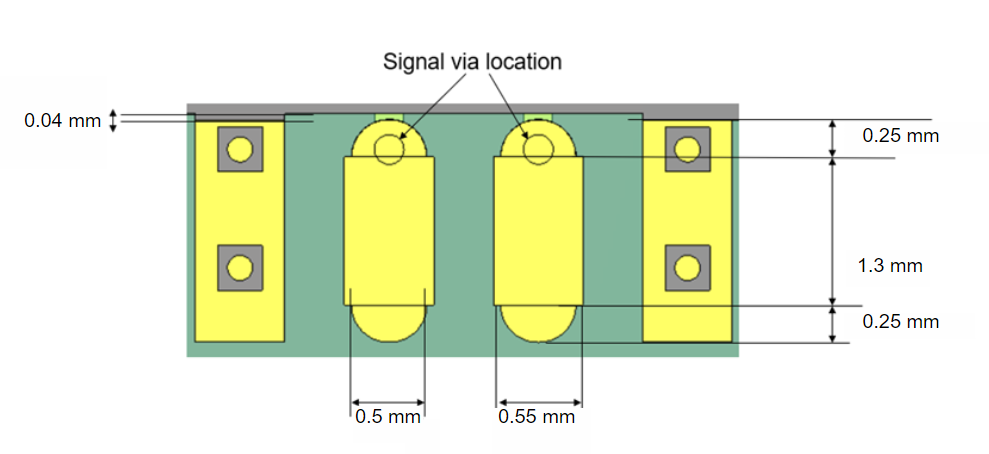 Figure 5. Add-in card stripline design of PCIe Gen7 CEM connector.
 Baseboard Design
Figure 6 illustrates the stripline footprint design employed in the baseboard/motherboard. In this design, the signal vias are placed at the north end of the pads. Another feature here is the skillfully rounded-off design of the pads on the north side. By rounding off the north end of the pads, the gap between the ground plane on the top layer and the north edge of the signal pads is minimized to a mere 0.06 mm.
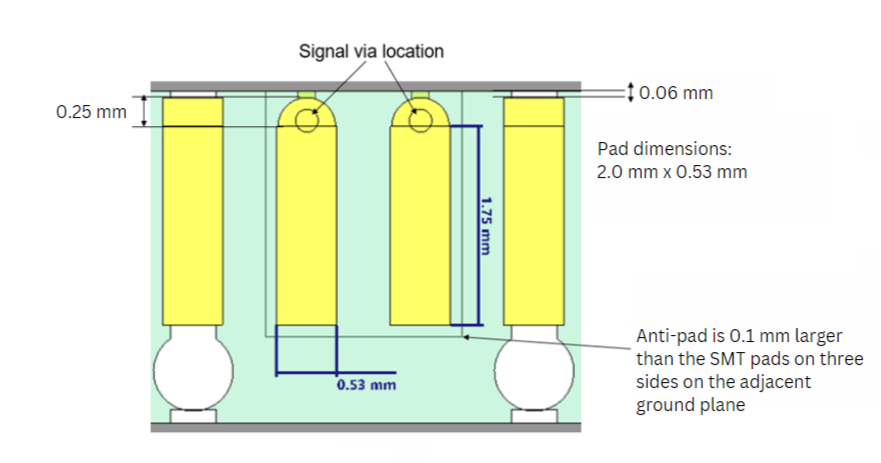 Figure 6. Baseboard stripline design of PCIe Gen7 CEM connector.
Conclusion
In summarizing our comprehensive analysis of PCIe Gen7 CEM connector designs, this article has shown the significant advantages conferred by the transition from a microstrip to a stripline footprint, particularly in the realms of SI performance for connector-only configurations. Our in-depth comparison reveals that the stripline footprint notably outperforms the microstrip in critical performance metrics, most prominently beyond the 24 GHz frequency threshold.
In terms of crosstalk, the stripline footprint demonstrated a significant improvement in FEXT, with 10.7% reduction in CCICN FEXT value stripline configuration underscores the enhanced crosstalk characteristics.
Our exploration of AIC design highlighted the strategic alterations made in pad dimensions, with a reduction in pad length from 2.5 mm to 1.8 mm and an increase in pad width from 0.5 mm to 0.55 mm. This modification countered the increased inductance caused by the shortened stub length by increasing mutual capacitance between signal pads.
The refined design of the stripline footprint in the baseboard/motherboard, further complements the improvements in SI. The precise rounding of the pads, particularly at the north end, and the optimal placement of signal vias, are crucial in minimizing the gap between the ground plane and the signal pads, thereby reducing potential resonance issues.
In conclusion, the transition to a stripline footprint for PCIe Gen7 CEM connectors presents a compelling case for its adoption in high-performance applications.
REFERENCES
- S. Smith and M. Rengarajan, "Overcoming the SI Challenges in Designing 25-40 Gb/s Backplane Channels," DesignCon, 2014.
- Y. Li, Y. Huang, A. S. Wander, A. Key, L. He, S. B. Smith, and Y. Zhou, "PCIe Gen. 5 CEM Connector and Add-In Card PCB Design Optimizations," in 2019 DesignCon, Santa Clara, CA, USA, Jan. 2019.
- PCI Express CEM Specification, Revision 5.0, Version 1.0.
- PCI Express CEM Specification, Revision 6.0, Version 0.5.
- PCIe Electrical Specification, Revision 7.0, Version 0.5.
- Abhijit Wander, “Navigating Signal Integrity Challenges: Transitioning from PCIe Gen6 to Gen7,” Signal Integrity Journal, February 2024.