
Introduction
DDR5, like many other memory technologies, is a parallel interface and requires advanced power sequencing, timing alignment, and receiver equalization training. DDR5 validation, therefore, is in-system and “as-configured.” One of the challenges of memory system validation is simply getting proper access to signals.
In-system testing requires a comprehensive array of solder-in probing and component interposer solutions. This article will outline various probe types and interposer solutions along with best practices for in-system measurements.
JEDEC defines DRAM voltage and timing limits at the DRAM package ball. To reduce lead inductance ball contacts for a package have been in use for many years. This has led to improved performance, but at the expense of testability. Due to this limited access, there are two options for capturing required signals. The first option is to probe directly at a nearby trace or via. Backside via probing is common for single-sided memory modules or even embedded systems. The second option is to attach a BGA interposer thereby tapping off relevant signals and routing out to an exposed pad.
High-frequency voltage probes used with oscilloscopes present various types of loading effects to the circuits to which they are attached.
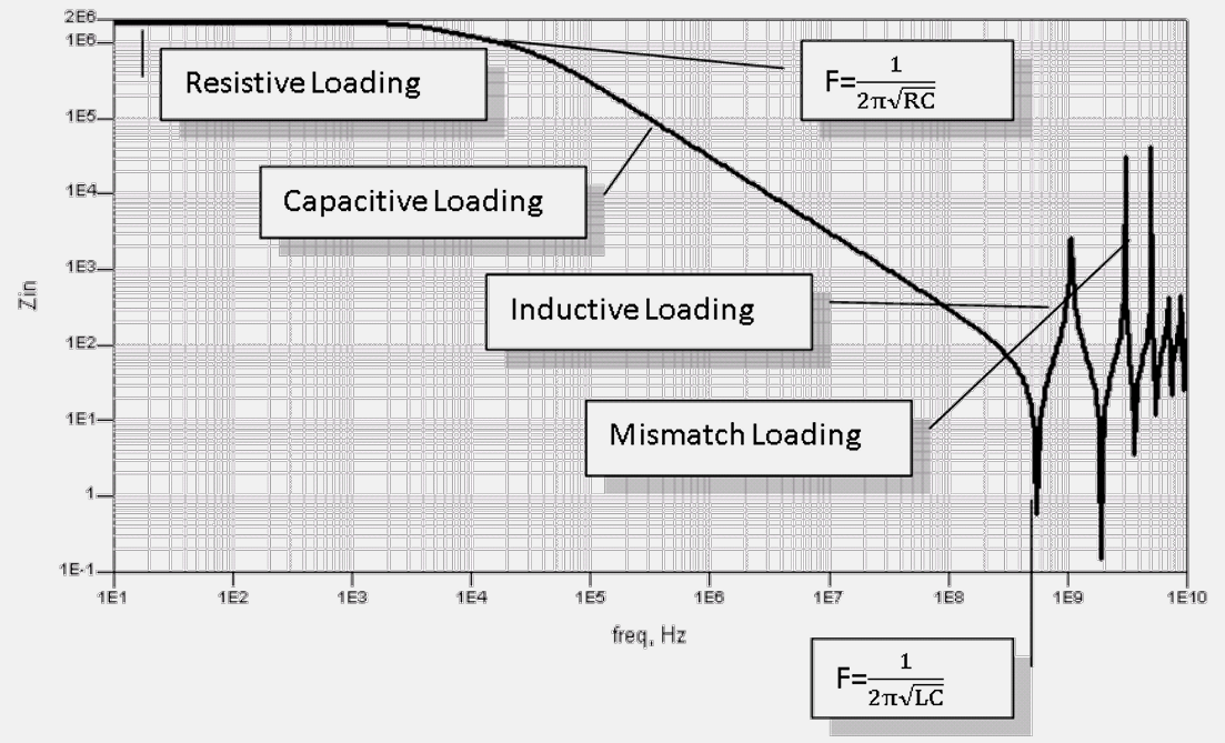
Resistive loading, primarily influenced by the probe’s input resistance, affects parameters like DC amplitude accuracy and bias voltage changes at DC and low frequencies. At higher frequencies, capacitive loading becomes significant due to decreasing probe capacitance impedance with rising frequency. This hampers bandwidth and signal edge speed, necessitating low-input capacitance designs.
Inductive loading dominates above the first resonance frequency and can distort signals if the LC resonance is within the probe's bandwidth. Inductive loading arises from loop inductance between the probe signal and ground tips, causing ringing in waveforms. Minimizing ground lead length is recommended to mitigate inductive loading.
High-bandwidth active probes prioritize mitigating capacitive and resistive loading effects in their design, crucial for high-accuracy probing in memory applications. Two common probe architectures, RC and RCRC input impedance, define their loading characteristics. RC probes maintain high impedance, reducing signal distortion across a broad frequency range. RCRC probes offer even higher impedance at very low and high frequencies, but lower midband impedance than RC probes.
Choosing the right probe depends on the signal's source impedance; RC suits high-impedance signals, whereas RCRC excels at reproducing fast-edge waveforms, but may affect voltage measurements with high source impedance or long time constants. Measuring a continuous signal such as a clock could benefit from a RCRC probe, whereas the most accurate signal reconstruction of bursted signals such as data (DQ) and strobe (DQS) is possible with RC probes.
The probe amplifier is one part of the probing system that buffers and drives the signal through a long cable before being received at the oscilloscope front end. The other side of this probing setup, which connects to the probe amplifier, is the probe tip or head. Figure 3 shows examples of various probe heads that might be used and for which applications these are better suited.
 Figure 3. Common interchangeable probe heads with varying geometries, performance, and usage.
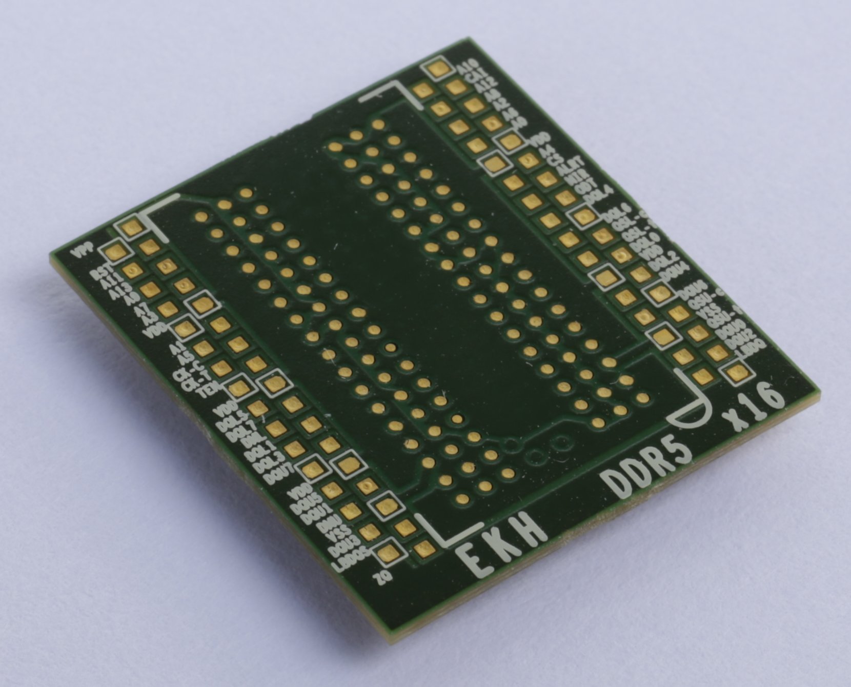
JEDEC electrical and timing measurements are taken at the ball of the DRAM package. But, as mentioned previously, the BGA ball is hidden underneath the package, which makes soldering a probe nearly impossible. A component interposer is needed to break out the high-speed signals and route them to a physically accessible pad for attaching a probe. In some cases, an additional PCB called a riser may be included to further elevate the interposer for better keep out volume. The keep out volume spacing is necessary for thermal management and mounting constraints.
 Figure 4. BGA component interposer and riser with various high-speed signals routed out to edge pads. (Image courtesy of Nexus Technology.)
 Some applications have tight keep-out volume or require volume testing of memory components with interposer reuse (socket form factor). Interposer suppliers can even design custom interposers for unique or specific requirements beyond traditional needs. If you have needs that existing interposer options cannot fulfill, contact your interposer supplier for a potential custom design.
 Figure 5. Various DRAM component interposer options including socketed and interposers with horizontal and vertical mounted solder pads. (Image courtesy of Nexus Technology.)
In addition to a BGA device interposer, a slot interposer is available for probing systems that have an Registered DIMM/Unbuffered DIMM (RDIMM/UDIMM) or Small Outline DIMM (SODIMM) connector. In this configuration, the signals are routed up from the socket on the motherboard through the interposer and up to a straddle-mount connector on the top of the slot interposer. The DIMM is then placed in the straddle-mount connector. The etch length is all carefully matched, and at boot time, the system trains with the extra etch length as part of the memory channel. Like the BGA interposer, a resistor/capacitor network is used to take a small amount of current off the bus and send it down a cable to be received by the logic analyzer. The RC network is placed on the signal to minimize stub loading and reflections, which is critical to be able to observe signals at the higher DDR5 speeds. This slot interposer and logic analyzer solution is ideally suited for system-level debug and validation.
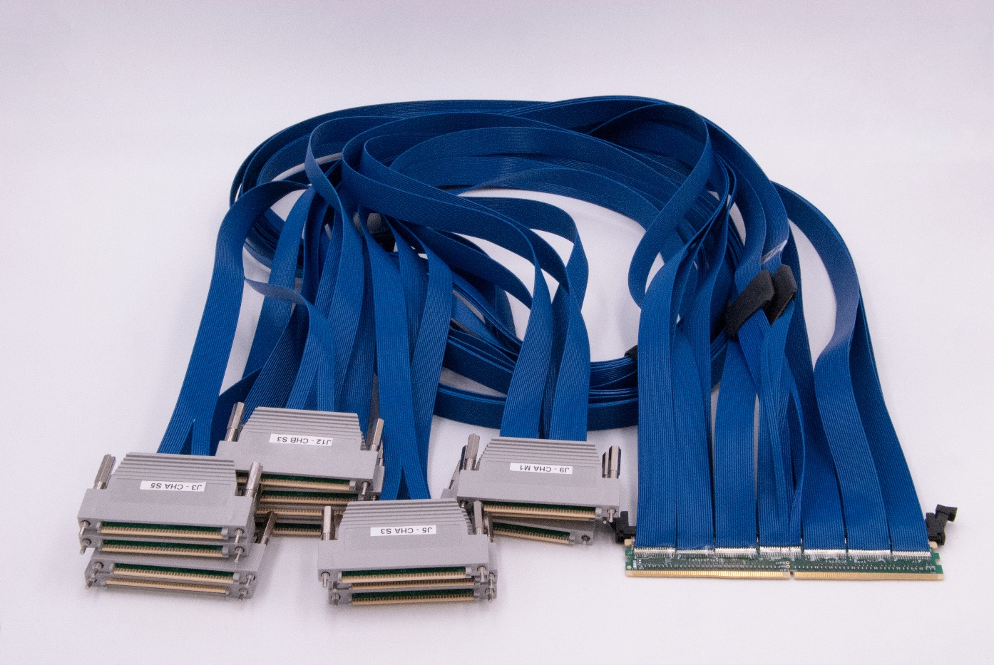 Figure 6. DDR5 RDIMM/LRDIMM Active Interposer. Note, ribbon cables route pickoff signals to Logic Analyzer. (Image courtesy of FuturePlus Systems.)
Best Practices for Attachment, Modeling, and Usage of Interposers and Probes
Now that we understand the role of an interposer while testing memory, let’s look at a typical process for how to attach a probe to a BGA interposer. The interposer attachment to the host board is outside the scope of this document. However, care must be taken when attaching the interposer to follow the supplier guidelines of pre-baking, reflow, and memory reattachment. The first step is to apply solder to the pads in preparation for attaching the probe tips.
 Figure 7. Attach interposer with proper reflow equipment.
It’s easier to attach the lead wires to the probe head than attach the wires to the pads. For optimum signal integrity, keep the wire length as short as possible. The shorter the wires, the less lead inductance, resulting in the highest performance measurements. In preparation for attaching the wires to the pads, it’s easiest to gently bend the wires to a nearly 90 degree angle, thus allowing for more surface contact and a more robust solder connection.
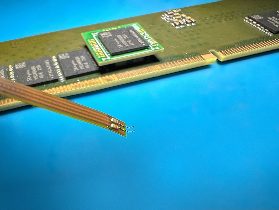 Figure 8. Prepare probe tip while bending wires for ease of connection.
Next, secure the probe head to the board in the best location prior to soldering the wires. This connection should be as robust as possible. Use double-sided tape, putty, or hot glue. It’s common, especially for flex cables, to have a full ground plane on one side to shield from noise and interference. Make sure to attach this shield plane towards the board. In addition, arc the probe tip away from the board vertically for the best signal fidelity. Add flux to the pads and reflow the solder to attach the wires to the pads.
 Figure 9. Attach probe head while maintaining vertical orientation.
 Lastly, add other probe connections following the same process as above. With higher density of connections, it might be necessary to adjust the angle of connection or the wire length.
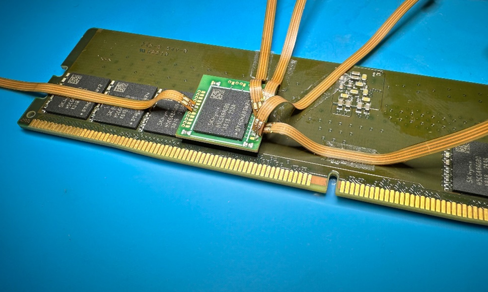 Figure 10. Additional probe heads attached with proper spacing.
Test Equipment Loading
As discussed in Figure 2, a probe and interposer will present some non-ideal loading to the circuit which is being measured. This loading is typically modeled as shunt capacitance. Most high bandwidth probes list the typical input capacitance (typical) in their data sheet. These can range from a few hundred fF to a few pF. This doesn’t seem like a lot of loading, but whether this will disturb the system operation or not depends on a few factors. First, consider the orientation of the probe relative to the board and it’s mutual coupling. Some probe suppliers even provide correction filters that are modeled based on either vertical or horizontal orientation. A vertical orientation is ideal and creates the least amount of capacitive coupling.
Next, the signaling type and corresponding frequency content is important. A clock, for example, is typically generated as a continuous signal, and for an assumed 50% duty cycle, consists of only it’s fundamental and odd harmonic frequencies. The DQ and DQS signals, however, are bursted and include a wide range of spectral content. But more importantly, the concentration of spectral energy transitions between low and high frequency bands as the signals turn on and off. The uniform impedance profile of a RC probe is an advantage for bursted signals.
Based on these considerations, it can be difficult to properly judge expected loading from a data sheet or rule of thumb. It’s highly recommended to include probe and interposer loading models in a simulation to not only verify performance with test equipment loading included, but also, perhaps more importantly, assess the operational health of the system. Suppliers provide Spice or S-parameter models for this purpose.
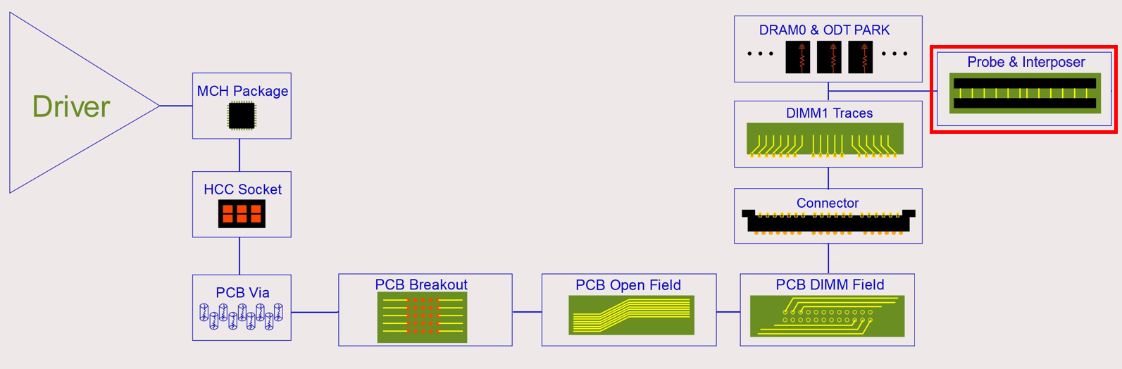 Figure 11. Example system design with interposer and probe model included.
Measurement De-embedding
Probe loading effects are removed in the oscilloscope software. The software simulates the unloaded probe response as an open circuit. In this way, the measurement setup is evaluated as if the probe was not included. Next, the interposer loading effects are removed. The simulation replaces the interposer model with an ideal through or short connection. In other words, the interposer is physically in-between ("inter-posing") the PCB and DRAM, but the measurement removes this connection and models the connection as a clean through path. For the measurement setup, the test equipment loading effects are removed to verify the true signaling behavior.
The models can vary for a probe and interposer. This depends on the use case, relevant connections, and signaling type used. For example, DQ and DQS signals are single-ended and differential, respectively. Therefore, each would use a model that represents the corresponding topology. See Table 1 below:
| Signal Name | Signaling Mode | Application | S-Parameter |
| DQ or CA | Single-ended | Simulation | 2-port (Host-DRAM) |
| DQ or CA | Single-ended | Measurement | 3-port (Host-DRAM-probe) |
| DQS or CK | Differential | Simulation | 4-port (Host-DRAM) |
| DQS or CK | Differential | Measurement | 6-port (Host-DRAM-probe) |
Table 1. Interposer signal path models for various signals and applications.
Removing probe loading is the next step. Generally, a probe is represented by a 1-port model. This model provides the frequency depending on loading (impedance) as seen by the circuit under test. With frequency dependent models, make sure to control the post-processing gain (low-pass filter). More gain is expected to be applied where more loss occurs at higher frequency. But the actual high frequency energy present in the signal will decrease to the point where applying gain will increase noise more than signal.
The following section provides an example of probe and interposer de-embedding. This is UDIMM system with the interposer attached to one of the DRAMs. There are several probes attached, but only the data signal is being analyzed.
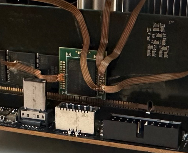 Figure 12. DDR5 system with BGA interposer and probes attached.
The de-embedding setup requires the user to define the system so the software knows how to apply the correction filter. For simplicity, this setup does not include specific driver or load settings such as on-resistance, on-die termination, or package definition.
 Figure 13. De-embedding configuration with measurement and simulation setup defined.
 Using a memory exerciser application, test patterns are generated and the data signal is captured. In Figure 14, channel 1, shown in yellow, displays the original, uncorrected waveform and corresponding eye measurement. Channel 2, shown in green, is the waveform after applying the de-embedding filter, which removes the probe loading and interposer effects. After de-embedding the eye height increases from 214.8 mV to 239.1 mV, about an 11% improvement.
 Figure 14. Before (yellow) and after (green) de-embedding of DDR5 interposer.
Summary
Optimizing DDR5 memory system validation involves a strategic focus on probe and interposer solutions for in-system measurements. The selection of probe architecture, whether RC or RCRC, plays a key role in managing probe loading. To make the right choice, evaluating source impedance and signal characteristics, especially for bursted signaling, is essential. As DDR5 continues to evolve at higher speeds and reach its top speed phase, integrating non-ideal loading modeling within simulations and effectively de-embedding probe and interposer effects become critical components of a comprehensive testing plan.
This article is part one of a three-part series on DDR5 electrical and timing measurement techniques. Please access part two of the series here.
REFERENCES
- DDR5 DRAM Standard, JESD79-5B_V1, JEDEC, September 20, 2022.
- DDR5 x16 Interposer, Eyeknowhow.
- Demystifying RCRC and RC Probes, Keysight, 2021.
- DDR5 x4/x8 XH Series EdgeProbe Interposers, Nexus.
- FS2600A DIMM Interposer, Future Plus Systems.