
This article is part two of a three-part series on DDR5 electrical and timing measurement techniques. Please access part one of the series here.
Introduction
What is Clock Jitter?
Clock jitter is the timing variations of a clock from their ideal locations. Jitter in clock signals is typically caused by thermal noise, power supply variations, loading conditions, device noise, and interference coupled from nearby circuits. All DRAM input command and address signals are synchronous to the clock and the clock jitter must therefore be within the limits prescribed by Joint Electron Device Engineering Council (JEDEC).
The clock is driven to the DRAM by the registering clock driver for load reduced/registered modules, host for unbuffered/small outline modules or clock driver for clock driver unbuffered/small outline modules. Because the clock is measured within a system a high impedance, a solder-in probe is used to capture the clock signal. It’s important to measure as close as possible to the DRAM thereby observing the signal as close to the termination as possible.
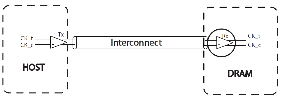 Figure 1. Input clock jitter measured as close to the DRAM as possible.
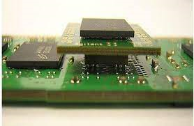 Figure 2. Using a BGA interposer to provide access to clock signal (also could probe a backside via).
Clock Jitter Test = N-UI Jitter
The clock jitter is evaluated across a moving window of N unit intervals. A unit interval for double data rate clocking includes both rising and falling edges. The Taccumulated_jitter or N-UI jitter is defined below.
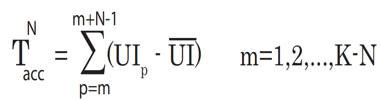 Figure 3. Accumulated or N-UI jitter definition.
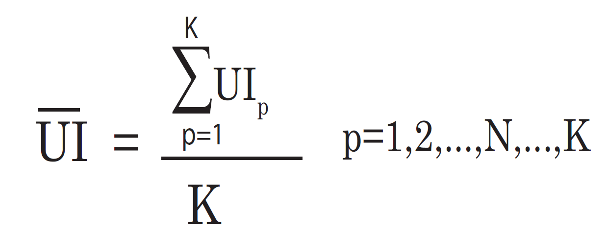
Figure 4. Unit Interval (UI) definition.
The sliding analysis window of N = 1, for example, might reference the initial edge as rising and then next falling edge. The next analysis segment will have an initial falling edge followed by a rising edge.
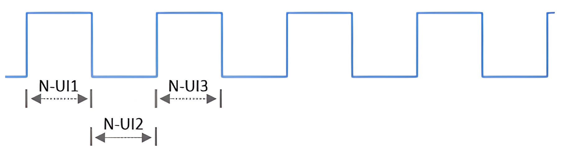 Figure 5. N-UI sliding window for N= 1.
With N = 4, as an example, the even number of UIs compares the same edge polarity 4 UI away across a sliding window.
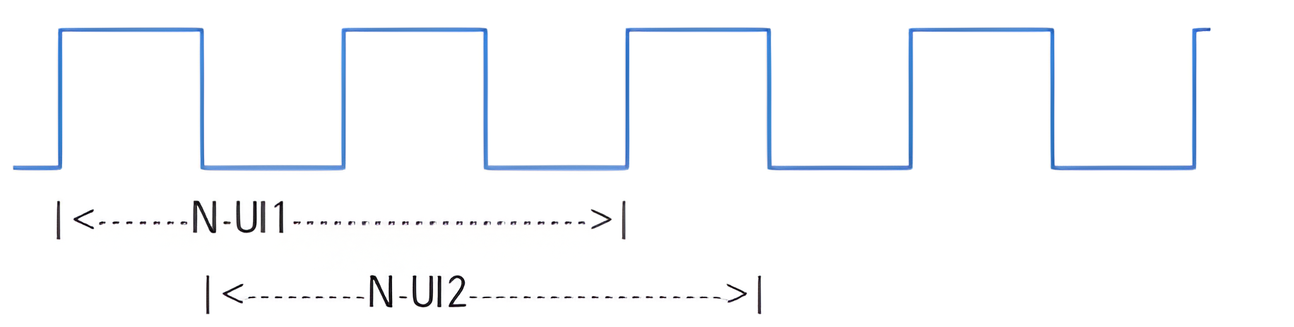
Figure 6. N-UI sliding window for N = 4.
Odd vs. Even N-UI Jitter
N-UI jitter is defined as the difference between the time of an edge, and another edge N unit intervals away relative to a known reference. Here, the unit-interval is defined as it would be for a data waveform, meaning that a clock is considered a data waveform with pattern [1 0], and the unit-interval is half of the pattern length (the length of a 1 or a zero). In this analysis, Duty Cycle Distortion (DCD) will always be zero for even N, and will return the same, non-zero value for odd N. Here’s an example:
 Figure 7. Example waveform for comparing even and odd jitter.
For N-UI jitter, with N = 1, we can assign the jitter to the first rising edge as j1 = t2 – t1 and assign the jitter to the first falling edge as j2 = t3 - t2. If there is DCD, then these will have different values, j1 is not equal to j2. Thus, the average jitter on all rising edges will not be the same as the average jitter of the falling edges, so DCD > 0.
Note, the jitter being referenced here does not include random jitter (RJ) effects as the averaging effects removes RJ effects but also given the jitter is grouped by rising and falling edges this corresponds to just DCD jitter. So DCD will be non-zero for all odd N.
For N = 2, assign the jitter to the first rising edge as j1 = t3 - t1, and on the first falling edge as j2 = t4 - t2. If there is only DCD, then the average jitter for rising edges will be zero, as will the average jitter for all falling edges, so DCD = 0. And this is true for all even N. This is why you might observe even N-UI jitter that is smaller than odd N-UI jitter.
Jitter Limits and Specification Table Notes
Unless otherwise noted, all jitter specifications are referenced to BER of 1E-16. This is important for TJ, as this requires any jitter analysis application to be configured with 1E-16 BER level.
The RJ specification of 3.7 mUI can be difficult to measure accurately and reliably without a few considerations. First, as will be shown later, the low RJ jitter limit has been approaching the jitter measurement floor of test equipment, and this requires removing the intrinsic oscilloscope RJ from the measured result. Because RJ is an RMS based parameter, this mathematical operation is done through a root sum square (RSS) subtraction process:
Signal_RJ = √ (Measured_RJ2 – Scope_RJ2)
The scope RJ is a function of the slew-rate based voltage noise converted to timing jitter. The equation used to calculate the effective scope RJ is based on the Period Jitter formula listed in the oscilloscope user manual. Note, the Period Jitter Measurement Floor equation is used due to the two-edge model of a clock period. These two edges correspond to the √2 term in the equation:
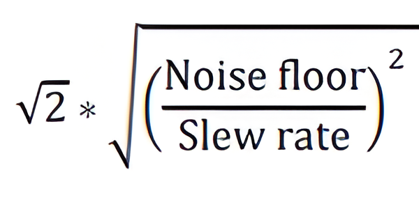 Figure 8. N-UI Jitter Measurement Floor equation.
Best Practices
Probe Calibration/Deskew
Calibration of a solder-in probe consists of a vertical calibration and a skew calibration. The vertical calibration should be performed before the skew calibration. Both calibrations should be performed for best probe measurement performance.
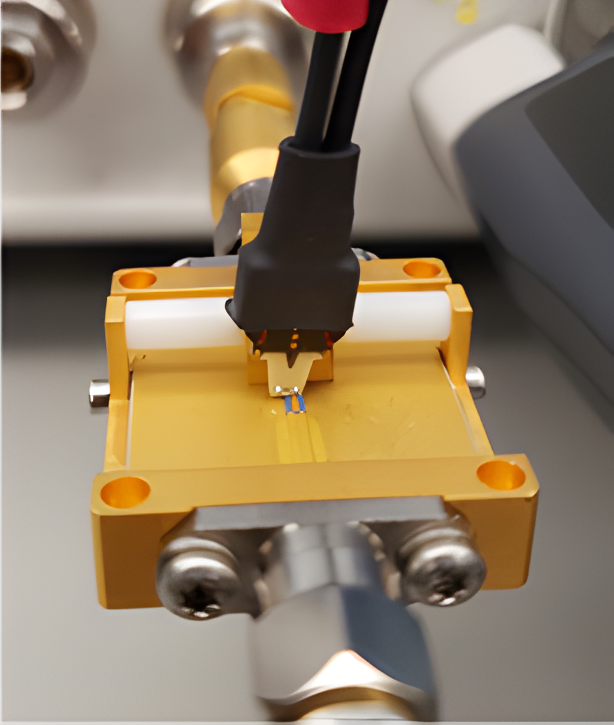 Figure 9. Example probe connection with probe + connected to center conductor and probe—to ground plane
After the DC gain/offset calibration has been performed, use the same setup to perform the skew calibration.
Random Jitter Removal
By measuring the oscilloscope noise and slew rate, the oscilloscope can calculate the oscilloscope's contributions to jitter and remove it from the reported RJ measurement.
You will be asked to remove your probe from the oscilloscope's input while calibration takes place and to reconnect your probe when finished. But since the probe amplifier contributes some noise to the overall instrument setup, the probe amplifier should remain attached to the scope input. Disconnect the probe head from the amp to isolate any residual signal noise from the scope noise calibration.
Automatic calibration of oscilloscope jitter works by measuring the AC Vrms of the baseline instrument noise level. This AC Vrms should be evaluated at the same location where the measurement threshold will be set to during the actual jitter measurement. Next, you need the slew rate between the threshold upper and lower limit of the data signal. The slew rate is measured during the jitter measurement process. With these values, the jitter measurement floor is computed based upon the performance characteristics equations published in the oscilloscope data sheet. This yields the oscilloscope's random jitter, which can then be removed from the reported RJ and TJ based on the equation below. The calculated oscilloscope RJ is also reported in the jitter results.
Bandwidth Control
The measured RJ highly depends upon the oscilloscope bandwidth used. Too much bandwidth and you will likely introduce more out-of-band noise and higher RJ. Not enough bandwidth may result in an unrealistic setup that doesn’t match real-world performance. JEDEC does not prescribe oscilloscope measurement bandwidth when making clock jitter measurements, so it’s up to the user to determine what setting is relevant. One should consider the actual DRAM receiver performance (e.g. VGA bandwidth) and accompanying channel frequency-dependent loss profile. This should be balanced with ensuring consistent slew rate performance.
You can visually check the high frequency content present in the signal by turning on a frequency domain view. If the signal power is below 30 or 40 dB, then this frequency might be a good place to limit the bandwidth. To minimize the addition of aliased noise, you should always use the max oscilloscope sample rate, regardless of the bandwidth setting.
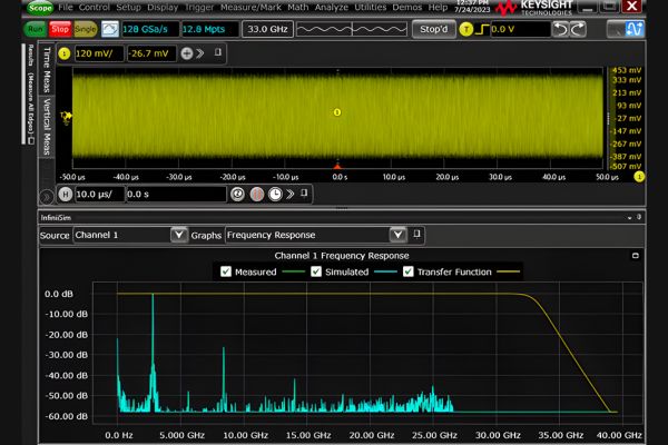 Figure 10. View FFT to compare actual signal energy for determining ideal bandwidth setting.
DDR5 Input Clock Jitter Test Procedure
The following outlines specific steps to measure DDR5 input clock jitter using a jitter/noise analysis application.
1. Perform oscilloscope and probe calibrations, if not already previously done.
2. Attach a probe as close to DRAM input as possible using interposer or other appropriate signal access solution. Minimize wire length as much as possible to reduce lead inductance.
 Figure 11. Probe head attached to BGA interposer.
3. Initialize system to start transmitting the clock. If possible, set adjacent lanes to static (DC) levels.
4. Adjust vertical scale and offset to fit signal on screen centered and with largest range on screen.
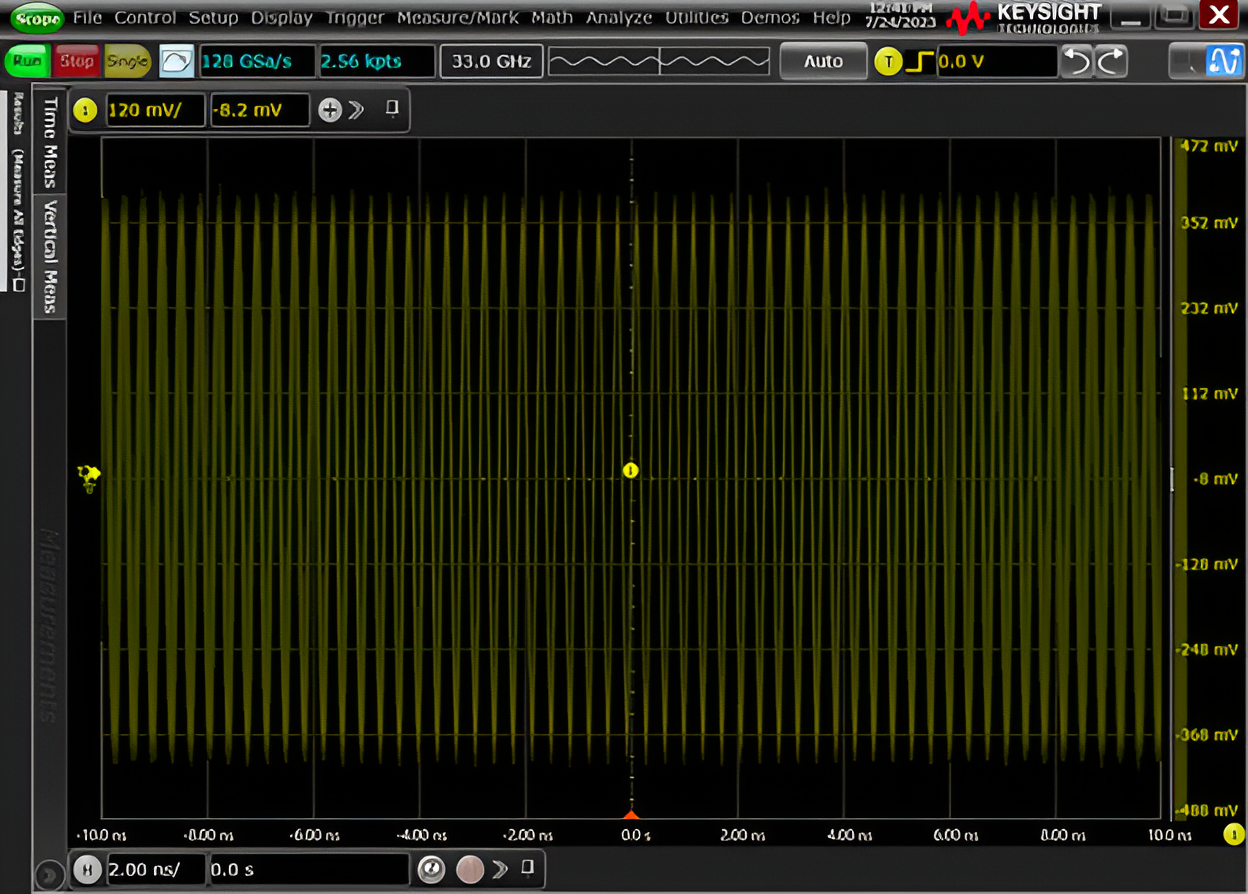 Figure 12. Differential clock optimally positioned on screen.
5. Adjust horizontal scale to capture at least 1M UI (10 µs/div or more).
6. Adjust channel bandwidth to the appropriate setting. The bandwidth can be set in Setup -> Bandwidth Limit.
For this example of DDR5-5600, the ideal bandwidth has been determined to be 10 GHz.
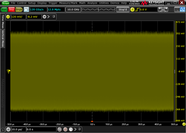 Figure 13. Capture at least 1M UI with 10 µs/div or longer.
7. Go to Remove RJ menu (Analyze -> Jitter/Noise -> Advanced -> Remove, Specify Jitter, Noise). In the Remove Scope Random Jitter section, select Automatic. Press Calibrate scope jitter/noise.
(Note, if this is the first time you are running the Calibrate scope jitter/noise, you may be asked to run the jitter wizard first. The wizard can help to optimize the vertical & horizontal scales, memory depth, clock recovery, etc.)
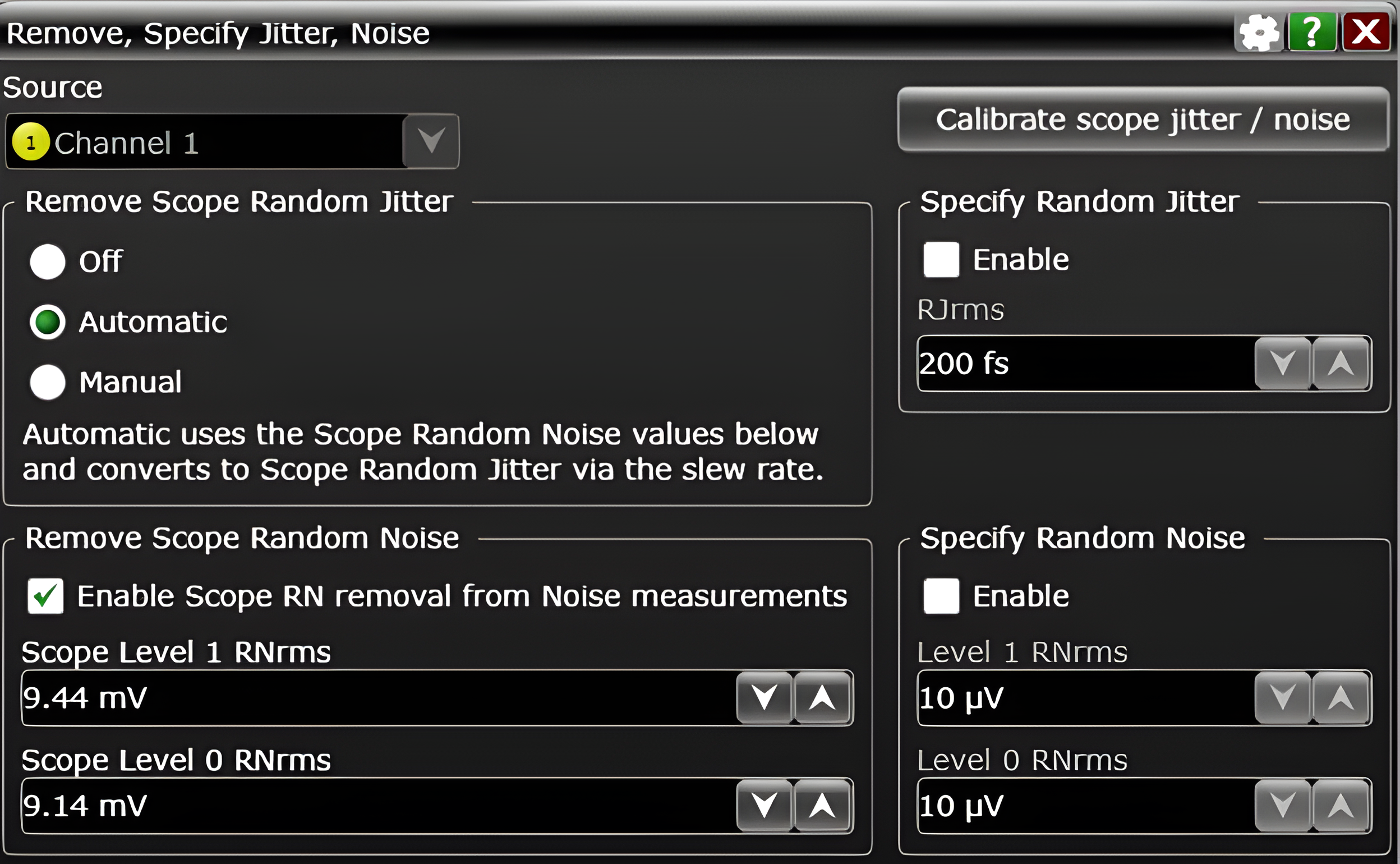 Figure 14. Remove Scope Random Jitter configuration menu.
 8. Disconnect probe head and leave probe amplifier attached to oscilloscope channel input.
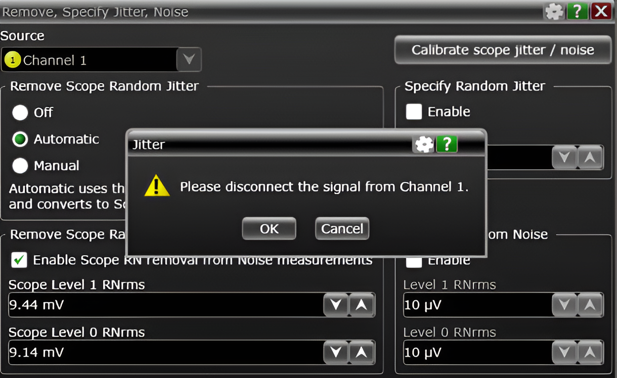 Figure 15. Prompt for disconnecting signal during noise profile calibration.
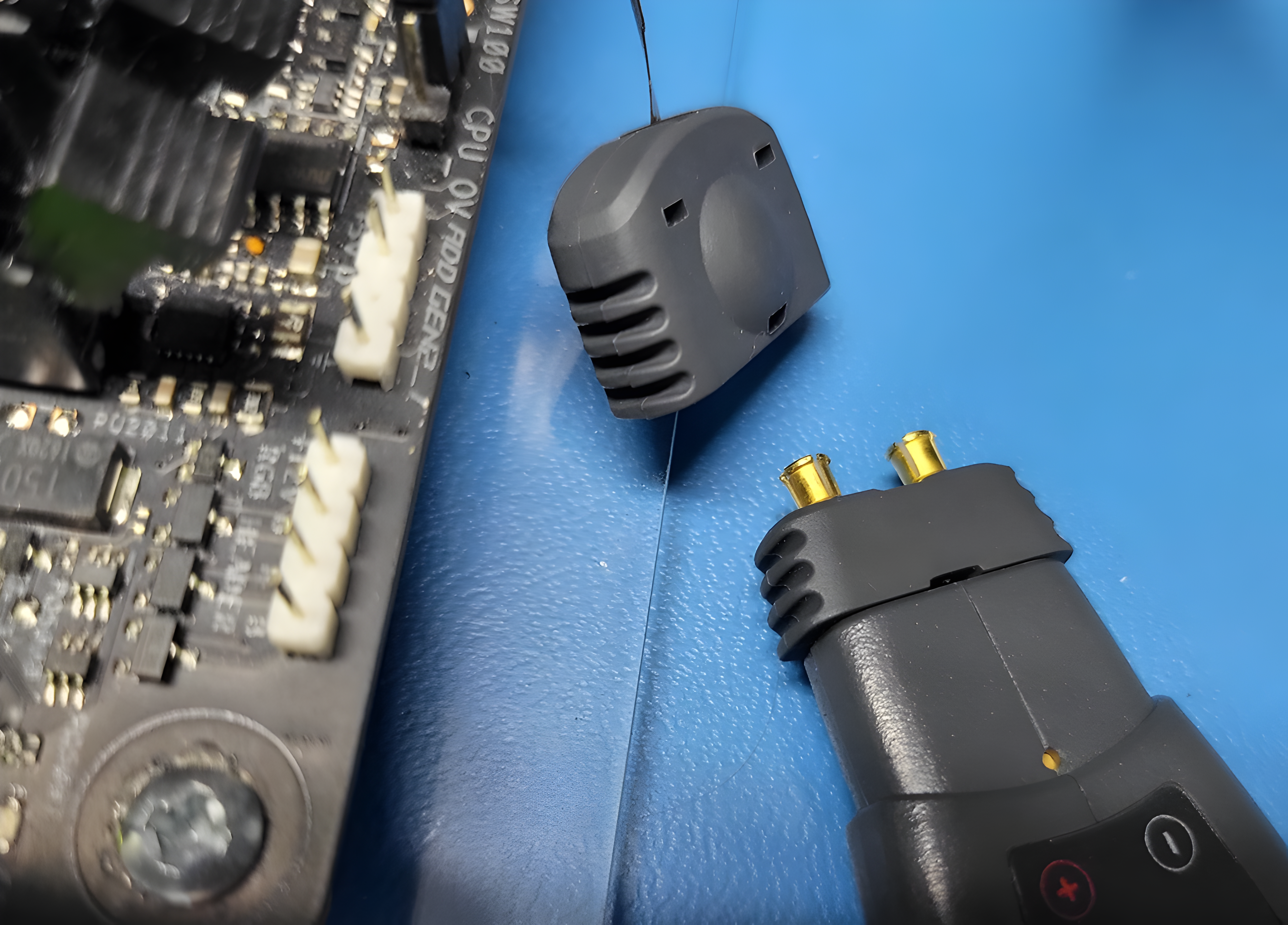 Figure 16. Disconnect signal from scope input by leaving probe amplifier connected to scope and disconnecting at probe head side.
9. Once you see the Calibration Complete message box, reattach the probe amplifier back to the probe head.
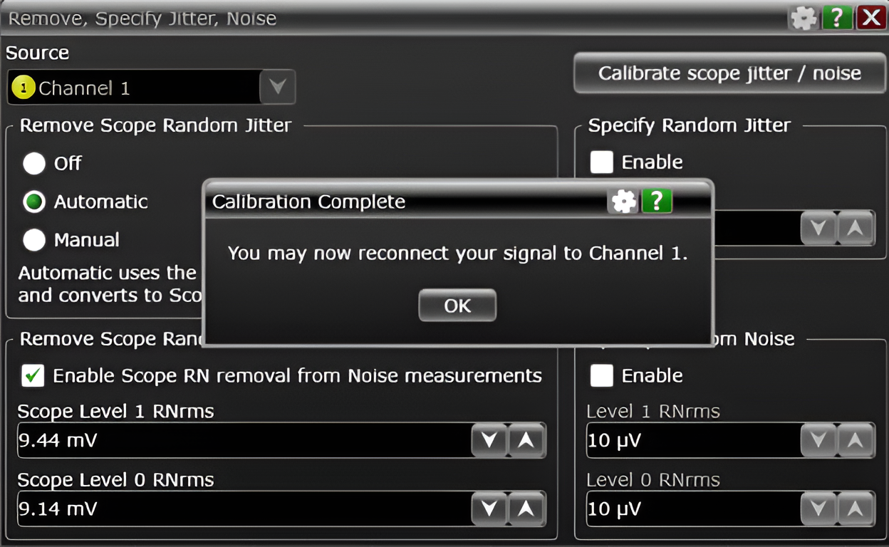 Figure 17. Reconnect probe head after noise profile is measured.
10. Return to Jitter/Noise Setup menu.
11. Configure the app with the following settings:
- Set Threshold to 0 with appropriate hysteresis levels (use "Auto," if needed).
- Clock recovery = constant frequency.
- BER Level = 1E-16.
- Pattern Length = Period with Auto checked.
12. Check Enable checkbox, then configure these additional settings:
- Spectral & Tail Fit -> Report Tail Fit.
- Display Units = Unit Interval.
- Edges = Both.
- N = 1. (Later, advance to N = 2, 3, …30)
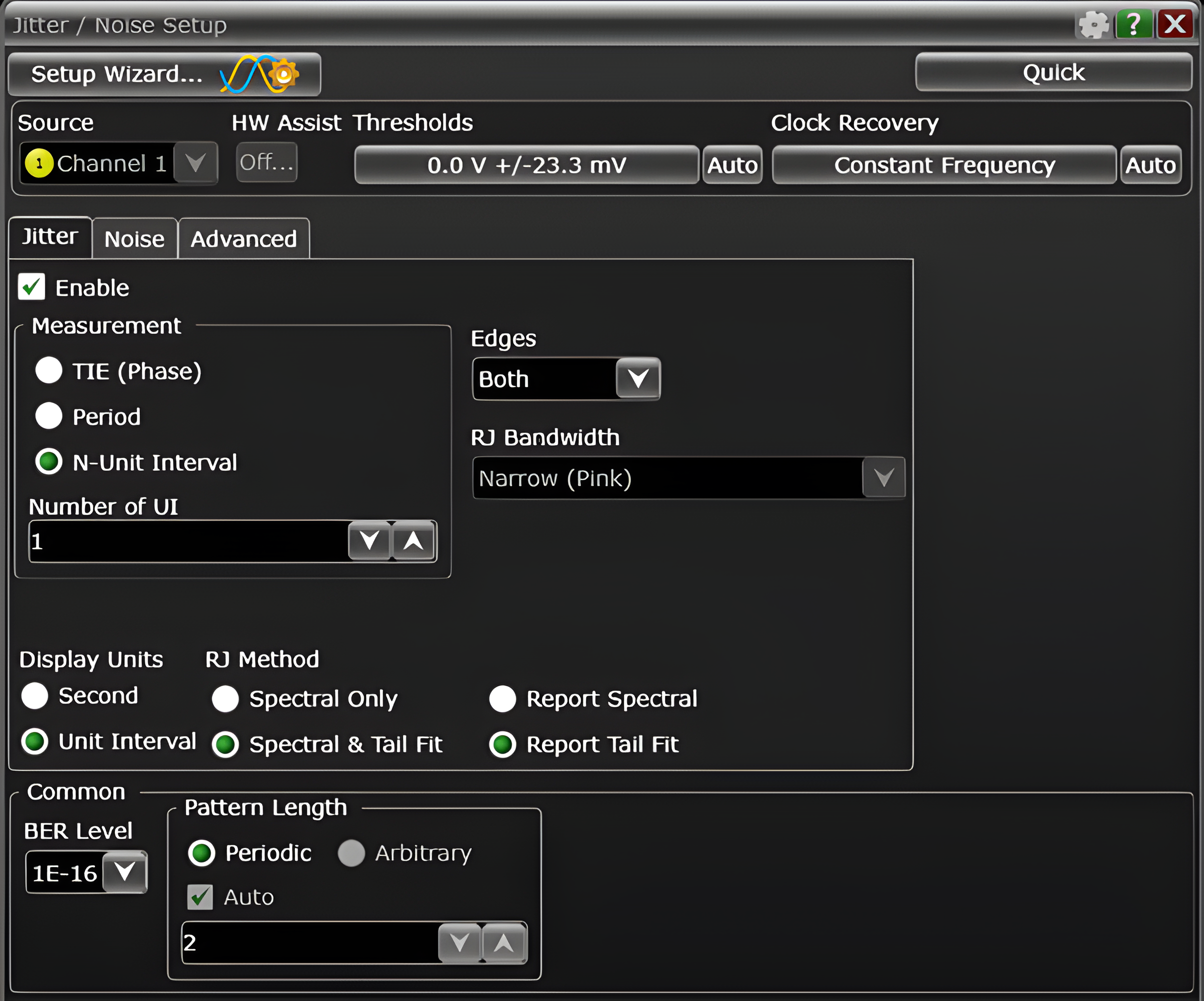 Figure 18. Final EZJIT configuration.
13. Press the clear button to remove any previous results and waveform data.
 Figure 19. Clear Display/Data button.
14. Run or single to acquire new signal.
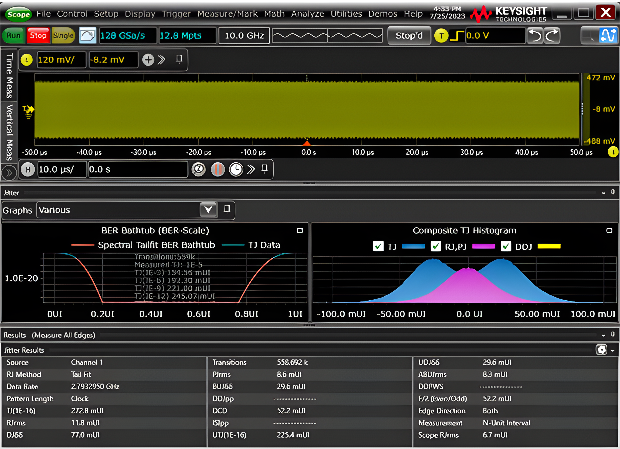 Figure 20. Results table with BER bathtub and histogram plots.
Note, DCD is present, but UDJdd does not include BUJ, which meets the requirement to not include BUJ for DDR5 clock jitter tests. Also, RJ is BUJ independent with Tail Fit.
Use the UTJ(1E-16) value to determine the TJ (no BUJ) measurement result.
The final results from this DDR5-5600 example are:
- Rj RMS value of 1-UI Jitter = 11.8 mUI (2.1 ps)
- Dj value of 1-UI Jitter = 29.6 mUI (5.3 ps)
- Tj value of 1-UI Jitter = 225.4 mUI (40 ps)
Summary
In this article, we discussed variations in clock timing and how this can impact the reliability of a memory system. The DDR5 standard prescribes very tight limits on random, deterministic, and total jitter. This jitter is measured across a moving window of N unit intervals, thus evaluating various forms of short-term jitter. It’s important to consider probe calibration, RJ removal, and controlling bandwidth for accurate measurements. As the example has shown, care must be taken during probe attachment, calibration, and using a jitter/noise analysis application to evaluate jitter levels, ensuring memory reliability.
REFERENCES