
What is USB4 Version 2.0
The USB-IF released the USB4 Version 2.0 Specification in October 2022. With this latest specification, each link will have four bidirectional differential lanes, and each lane will run at 25.6 Giga Baud (GBd), 40 Gb/s. In the symmetric mode, each link will have two lanes running at 40 Gb/s for an aggregate 80 Gb/s in each direction. With a new asymmetric mode, the link can be negotiated to transmit three lanes in one direction. The net result is 120 Gb/s in one direction, and 40 Gb/s in the other direction in asymmetric mode.
To increase and double bandwidth, this next-generation USB technology chooses PAM3 at 25.6 GBd and 40 Gb/s using 11 bit/17 trit encoding. This small increase in the fundamental frequency from 10 to 12.8 GHz allowed the use of existing USB4 and Thunderbolt 4 cables and connectors. For PHY layer electrical validation engineers, each of the four differential pairs will run at 25.6 GBd, PAM3, and 40 Gb/s. Figure 1. USB4 Gen4 compliance test point definitions.
USB4 Version 2.0 Simulation
The cost of turning silicon is very high, plus it adds delays to a first to market strategy. A key component of reducing this risk and increasing success is to perform rigorous end-end simulation of the entire USB 80 Gb/s link. To enable early design stage simulations as well as extensive system level post-layout analysis, simulation solutions for USB4 Version 2.0 that incorporate IBIS-AMI model makers facilitate the development of such models for USB 80Gb/s devices. These IBIS-AMI models are then used in channel simulations to predict and simulate the BER, eye metrics, and other design parameters.
With USB 80 Gb/s PAM3, signal and power integrity are critical as frequency and speed increase in PCBs. Losses associated with transmission line effects will cause failures in Gen 4 devices. It will be crucial to model traces, vias, and interconnects to simulate the board accurately. Plus, improve high-speed link performance in PCB designs with integrated circuit design and electromagnetic simulators customized for power and signal integrity analysis. Figure 2. USB4 Version 2.0 TX and RX Return Loss test limit requirement.
USB4 Version 2.0 Transmitter Testing Fundamentals
To ensure precise TX characterization, there are a couple of key Test Points (TP) that need to be well understood. TP2 is defined at the output of the compliance test fixture and where all TX measurements are performed. What is different from Gen 2/3 is there are no longer measurements performed at TP3 for Gen 4. However, a captive/tethered cable device measurement is always performed at TP3 because the only accessible measurement point is at TP3.
There are the traditional jitter and timing measurements from Gen 2/3, but now performed on a PAM3 signal. As mentioned above, the most significant challenge with Gen 4 is the vertical signal margin. Hence, there are a number of new vertical measurements introduced with Gen 4 to ensure acceptable BER performance.
Level_Mismatch compares the difference in eye opening between the “top” and “bottom” PAM3 eye. Using linear fit pulse response, sigma n, and signal e, SNDR (Signal Noise Distortion Ratio) is another key vertical margin parameter. Integrated Return Loss (IRL) takes into account the signal quality at the transmitter coupled with the insertion loss of the channel for another important vertical margin parameter.
Gen 2/3 had 16 TX presets. To no surprise, Gen 4 with more loss has 42 presets. Just like Gen 2/3, a sweep needs to be performed on all 42 presets to characterize each individually as well as to determine the optimal reset for minimum data-dependent jitter.
If a USB 80 Gb/s product is anything larger than a USB stick, there is a high likelihood a re-timer is required. This requires clock-switch measurement like the frequency variation training measurement.
USB4 Version 2.0 Receiver Testing Fundamentals
Like Gen 2/3, Gen 4 has the typical stress cocktail components such as launch voltage, ACCM, PJ, RJ, and loss channel.
Like Gen 4 TX, Gen 4 Rx introduces new vertical stress components like SNDR, Level Mismatch, DMSI, and CMSI.
Like Gen 2/3, there are the two use and test cases:
- Short channel for low loss products or link partners connected with active cable
- Long channel for link partners connected with a passive cable.
Gen 4 added a third use and test case for link partners connected to a linear redriver cable. Similarly to Gen 4 TX, there is also a special test case for tethered/captive devices. The draft version of the CTS requires that aggressors be added for RX testing.
Additional Test Requirements for USB4 Version 2.0
Similarly to Gen2/3, side-band testing will be required to ensure proper link negotiation. New requirements for TX and RX LFPS testing are planned to be introduced with Gen 4. As mentioned above, Gen 4 added an asymmetric operation mode that also requires specialized testing. It cannot be stressed enough that vertical margin will be challenging. Hence, the test methods require noise compensation to reduce the effects of measurement noise in the test system.
USB4 Version 2.0 Transmitter and Receiver Return Loss
USB4 Gen 2/3 introduced new differential and common mode return loss requirement for transmitter and receiver. This is carried on in Gen 4. Return loss, the ratio of reflective power to incident power, is the direct measure of the impedance match of a transmission line. Meeting the test limit requirement is critical to meet compliance certification and ensuring product performance and interoperability.
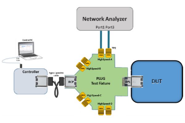 Figure 3. USB4 Version 2.0 TX and RX Return Loss proposed test setup.
In USB4 Version 2.0, the IRL measurement was introduced, and the differential return loss requirement remains one of the informative items for compliance certification. The increased bit rates to 80 Gb/s to support USB4 Version 2.0 protocol introduce additional signal integrity challenges and require a more stringent integrated (summed) return loss test corresponding to the integrated power spectral density of the incidental/reflective behaviors over the baseline baud rate frequency range.
The transmitter IRL is extracted as follows: 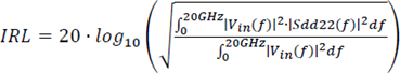
- Sdd22(ƒ) is the Return-Loss of the transmitter at TP2, referenced to single-ended load impedance of 42.5 Ω
- Vin(ƒ) is the spectrum of the ideal PAM signal with a 20% slew rate, defined as
- Viin(ƒ)=sin (π∙ƒ∙Tr) / π∙ƒ∙Tr * sin (π∙ƒ∙Tb) / (π∙ƒ∙Tb, with Tb=39.0625ps and Tr=0.2∙Tb
The transmitter and receiver differential return loss (Sdd22) and integrated return loss (IRL) will be setup as below. An S-Parameter touchstone file (S2P) will be measured by a Vector Network Analyzer (VNA) while the transmitter/receiver DUT is in active mode with PRBS7 pattern driving by a USB4 test microcontroller and ETT tool. The measured S-Parameter will be analyzed by the SigTest tool for delivering test results.
The transmitter IRL maximum limit is a function of the measured transmitter ISI margin (TX_ISI_MARGIN) which corresponds to the transmitter signal-to-residual ISI ratio. Therefore, to verify the verdict of the transmitter IRL, a waveform file (.bin) of ui_jitter_vertical that is used in the transmitter’s timing and voltage measurement test will be compiled using the USB4 SigTest tool.
As discussed, in the transmitter and receiver return loss test, it may be possible in some cases for the TX or RX signaling of the DUT to introduce error into the measurement. Improperly configured DUTs (such as the DUT is not transmitting the proper pattern, or being forced into the incorrect mode,) can produce erroneous measurement results, which could lead to false failures. Care should be taken to ensure that all sources of error have been minimized. Besides, a VNA used for the measurement should warm up and be calibrated as necessary with an electronic calibration module prior to the measurement. The VNA’s setup should follow proposed CTS requirements with Port 1 and Port 3 connected to the DUT with a sweep frequency range from 50MHz to 20GHz and an intermediate frequency bandwidth at least 1600 points to minimize the trace noise.
New Test Requirements for USB4 Gen 3 and Gen 4 Cables
Compared to the previous USB 3.2 Type-C CTS, USB Type-C CTS for USB4 is much more complex. The increased bit rates to 40 to 80 Gb/s to support USB4 and USB4 Version 2.0 protocol introduce additional signal integrity challenges and require more stringent integrated test parameters corresponding to the incidental/reflective behaviors over a frequency range.
The new Test Group B-8 and Test Group A-8 requirements are aimed at the integrated S-parameters (except for insertion loss and differential-to-common-mode conversion) to avoid the potential rejection of a functioning cable assembly that may fail the traditional S-parameters spec at a few frequencies. In the case of IRL, it now manages the reflection between the cable assembly and the rest of the system (host and device) with more IRL allowed if the cable loss is smaller.
Summary
USB Gen 2/3 at 10 to 20 Gb/s NRZ continues to be very challenging to implement. USB Gen 4 at 25.6 GBd PAM3, 40 Gb/s, 11 bit/7 trit encoding, coupled with asymmetric mode crosstalk and the same loss channel makes it exponentially more complicated.
The IP/PHY development kits, simulation solutions, and T&M solutions reviewed in this paper are the foundation required for silicon and system integrators to design compliant USB4 Version 2.0 products that meet strict interoperability requirements in the vast Type-C ecosystem.