
The thickness of copper traces is an important parameter for accurate impedance prediction. Copper thickness is usually specified in ounces per square foot. Most common thicknesses for inner layer traces are ½ and 1 oz foil. But field solvers expect an actual thickness dimension.
Most designers assume 0.7 mils (18 μm) thickness and 1.4 mils (36 μm) for ½ and 1 oz, respectively. But because of the price of copper, the copper you get from foil manufacturers will likely be the minimum thickness allowed under IPC-4562A. When you factor in the typical thickness after fabrication, the typical thickness can be 0.6 mils (15 μm) and 1.2 mils (30 μm). But the minimum thickness allowed under IPC-A-600G-3.2.4 is 0.45 mils (11.4 μm) and 0.98 mils (24.9 μm) for ½ oz and 1 oz, respectively.
Due to the nature of the etching process, the traces will usually be trapezoidal in shape. This is known as the etch factor (EF), as defined by IPC-A-600G. It is the ratio of the thickness (t) to half the difference between W1 and W2, shown in Figure 1.
Thus,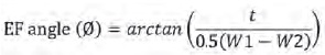 Some field solvers will define EF differently, so it is important to understand how to specify it properly.
Once you’ve come up with a proposed stackup, the next step is to do some impedance modeling. Normally your fab shop comes up with this, but it is a good idea to validate their proposal, to ensure you are in sync with them.
The first thing to do is identify the layers from which to model. Next, use your field solver to model characteristic impedance. Since all field solvers are different, and user interfaces can be confusing, make sure you understand the little nuances of your tool.
The next thing is to identify the core layers in the stackup and input H1 and Dk1 for the dielectric. Then, input the pressed thickness for prepreg H2 and Dk2, not the thickness found in Dk/Df construction tables. But be careful how the field solver defines H2. Most field solvers define it as shown in Figure 1, but some solvers, like Polar Si9000e, define H2 as the thickness of prepreg plus thickness of trace (H2+t), shown in Figure 2. Usually, you can trust the pressed thickness from your board shop stackup drawing.

Finally, if your field solver allows for it, fill in Dkresin between two traces if you know it. It will be lower than Dk2. Since this number is generally hard to obtain, a rough estimate to use is the lowest Dk value from the highest resin content prepreg found in Dk/Df construction tables. Once everything is set up, optimize the line width and space until the desired characteristic impedance is reached.
One last point to remember is that all 2D field solvers only calculate the lossless characteristic impedance. But when we measure an impedance test coupon with a time domain reflectometer (TDR), we are measuring the instantaneous impedance of a lossy transmission line at every point along its length. More often than not, impedance is different than what was predicted.
A 2D field solver has no input for conductor resistivity, dielectric loss, or the length of the conductor. Resistive loss often results in a slow monotonic rise in the impedance profile. IPC-TM-650 specifies the measurement zone between 30% to 70% and most PCB fab shops will measure an average impedance.
In the example, shown in Figure 2, for a low loss dielectric there is a 4 to 5 Ohm difference depending on where the measurement is taken. When all input parameters are included correctly for a lossy transmission line model, you can see there is excellent correlation.
Although minor differences in individual parameters may have second order affects, collectively they could add up to give poor correlation to measurements. But if you consider all the nuances discussed in this article, you can get pretty good accuracy as shown in Figure 2.