
To avoid “garbage in, garbage out” (GIGO) with any field solver, first you need to understand the little nuances of PCB fabrication processes and how to interpret manufacturers’ data sheets. But most importantly you need to understand the tool’s user interface and what it is asking for.
All 2D or 3D field solvers will give accurate impedance predictions. The differences are the type of solvers used under the hood and complexity of the user interface. Simple 2D field solvers, used in many of today’s stackup planners, simply give predicted characteristic impedance based on material properties and trace geometries. More complex, 2.5D or 3D field solvers, allow for additional material parameters and can also predict insertion loss, phase delay, and impedance over frequency. Some will even export RLGC and touchstone S-parameter files for further signal integrity analysis.
Standard PCBs are fabricated using cores and prepreg material. Prepreg sheets are a mixture of fiberglass (glass) cloth and resin which is partially cured. Cores are simply cured prepreg sheets with copper bonded to one or both sides of the laminate. Copper is etched away on each side of the foil to leave the circuit pattern.
In a multi-layer PCB, cores and prepreg sheets are alternately stacked symmetrically above and below the middle of the layup then pressed under heat and pressure. The prepreg layers get thinner when pressed allowing the resin to fill the voids between the copper features that were etched away on the cores.
One important parameter for accurate impedance modeling is dielectric constant (Dk). The best source is from laminate suppliers’ data sheets. But all data sheets from laminate suppliers are not the same.3
“Marketing” data sheets are data sheets easily found on laminate suppliers’ websites. They are meant for a quick comparison of dielectric properties to narrow your search for the right laminate for your application. They include mostly thermal and mechanical properties, which are important for the physical structure of the material and how it will perform with other material properties in the stackup during processing.
Marketing data sheets usually only report a typical Dk value at 50% resin content at two or three frequency points. Depending on glass style, resin content and thickness, Dk and dissipation factor (Df), will be different for different cores and prepreg thicknesses for the same laminate chemistry. In the end, they are not representative of what is needed to design an actual stackup, or to do impedance and loss modeling. Using these numbers will almost always lead to inaccurate impedance and signal integrity (SI) results.
Instead, you need to use the same Dk/Df construction table data sheets that PCB fabricators use for the stackup. Dk/Df construction tables provide the actual core and prepreg thicknesses, resin content, and Dk/Df for the different glass styles, over different frequencies. Depending on the stackup, a combination of thicknesses is often needed to meet impedance requirements and have different Dk values.
Many engineers assume Dk published is the intrinsic property of the material. But in fact, it is the effective Dk (Dkeff) measured by a specific industry standard test method. It does not guarantee the values directly correspond to design applications. When compared against measurements from a design application, there is often a discrepancy in Dkeff due to increased phase delay caused by surface roughness.1
Dkeff is highly dependent on the test apparatus and conditions of how it is measured. One popular test method, IPC-TM-650 2.5.5.5C clamped stripline resonator test method, assures consistency of product during fabrication. Due to the nature of this test method, the materials under test are not physically bonded together, air is entrapped between the various layers. These small air gaps are caused by: roughness of the copper foil plates in the fixture, roughness profile imprint left on the surface from the foil that was removed from the test samples, and copper removed on the resonant element pattern card. Air entrapment results in a lower Dkeff than what is measured because in a real PCB everything is bonded together, with no air entrapment.3
All glass weave reinforced laminates are anisotropic, which means E-field orientation, relative to the glass weave, is different depending on test method. E-fields produced from tests like IPC-TM-650 2.5.5.5C are transverse to the glass weave and Dkeff measured is out-of-plane.
E-fields produced by TM-650-2.5.5.13 split post cavity resonators are parallel to the glass weave Dkeff measured this way is in-plane. Dkeff is typically higher for in-plane measurements, compared to out-of-plane, depending on the glass resin mixtures used in the stackup.
Another source of discrepancy is not accounting for increased Dkeff due to the pressed thickness of prepreg. Since prepreg sheets have a certain percentage of resin content for the thickness, after pressing the resin content is reduced and since Dk is a function of resin and glass mixture, there will be a higher percentage of glass after pressing and thus slightly higher Dkeff.
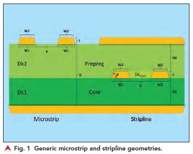 The most common PCB trace geometries are microstrip and stripline. A simple microstrip geometry is bare copper traces over a reference plane, separated by a dielectric height H, as shown in Figure 1. Depending on the stackup, there may be a core and prepreg layer between the outer layer and reference plane with the same or different Dk values for Dk1 and Dk2.
Simple stripline geometry has copper traces between two reference planes. For single-ended (SE) signals, there is only one trace used in the field solver to calculate the SE impedance. For differential pairs, there are two traces separated by a space. Because resin fills the voids between copper features the Dkresin will be lower than Dk1 or Dk2, shown in Figure 1.
The last thing to note is the wider side of the trace always faces the core material. This is a very important point to remember when using any field solver. If you get it reversed, it will lead to inaccurate results.