In high-speed circuit designs, power integrity (PI) and electromagnetic interference (EMI) are connected together. When the edge of the cavity created by power (PWR) and ground (GND) planes in PCBs radiates, the peak frequencies in the emissions are the same as the peak frequencies in the cavity self-impedance. This is because the high impedance of the cavity resonances will generate higher voltages from the return currents trapped in the cavity. It is these higher voltages that will drive the higher radiated emissions from the edge.
When the cavity is formed by two adjacent GND planes, the proper placement of ground return vias shorting the planes together can reduce the cavity impedance peaks and eliminate the noise source caused by the return current flowing between the planes. In this article, the placement of a ground via and the relationship between PI and EMI in a GND plane pair with a signal via passing through the cavity is outlined.
When a signal passes through a pair of adjacent GND planes, forming a cavity, the signal via provides a continuous path for the signal current. The return current must take a circuit-out path through the cavity. Between the cavity is an insulating dielectric. The only way for the return current to transfer from the top GND plane to the bottom GND plane is through displacement current. Once introduced in the cavity in the vicinity of the signal via, the displacement current propagate in the cavity, exciting EM resonances between the planes. When the propagating signal in the cavity reaches the edge, it has the potential of radiating as a line source. This is one way PI and EMI are related to each other.
To illustrate this effect, a simple model was constructed in HFSS. The cavity, (see Figure 1a) consisting of a 75 × 50 mm GND plane pair, 4.2 mils thick FR4 dielectric (εr = 4.5), and copper plane thickness of 1.2 mil is used as the test vehicle. A signal via (intended as noise source) is located at the center of the GND plane pairs and an optional ground via shorting the two GND planes is placed 50 mils away.
Figure 1b shows the simulated input impedance of the cavity at the location of the signal via and the 3 m emission (radiation from the edge of the GND planes) with/without the ground via. The input impedance is calculated by defining a discrete port across the antipad of the signal via.
Adding the ground via near the noise source is useful to keep the input impedance low and to mitigate EMI. As long as the distance between the signal via and the ground shorting via is fixed, the input impedance or the far-field emission frequencies are the same. The presence of the shorting via does not affect the reflections from the PCB edges via and the resonant frequencies. Similar results are obtained for other noise sources locations, as long as they are not too close to the edges and corners of the board.
As already mentioned, the edge of the plane pair acts as a line antenna and the equivalent circuit for the far-field estimation is shown in Figure 1. Zpp represents the GND plane impedance, Zin is the equivalent input impedance, Cport is the port capacitance (due to the antipad) and Zvia is the impedance of the shorting ground via. I is the displacement current, Iz is the current flowing on Zpp, and finally Iz’ identifies the current on Zpp after the ground via is added to the model.
From the analysis of the equivalent circuit the following equations can be extracted:
Iz = ZcapZcap + ZppI
Zin = Zpp//Zcap = ZcapZppZcap + Zpp
Zcap=1jωCport
Iz ’ = Zvia//ZcapZpp + Zvia//ZcapI
Zin’ = Zpp//Zcap//Zvia = ZcapZpp
ZviaZcapZpp + ZppZvia + ZviaZcap
Since the far-field (FF) is proportional to the current flowing on Zpp, we can obtain this relationship FF’/FF = Iz ’/Iz = Zin’/Zin which can be used to estimate the far-field strength before and after adding a shorting via and/or decoupling capacitor. A reasonable correlation can be observed for the frequencies of the impedance peaks and emission peaks and reduction in impedance peaks and reduction in far-field emissions with and without the shorting via.
In this example, only the cavity mode at 2.8 and 4.7 GHz radiate from the edge. This study demonstrates the importance of PI-EMI coanalysis when designing PCBs.
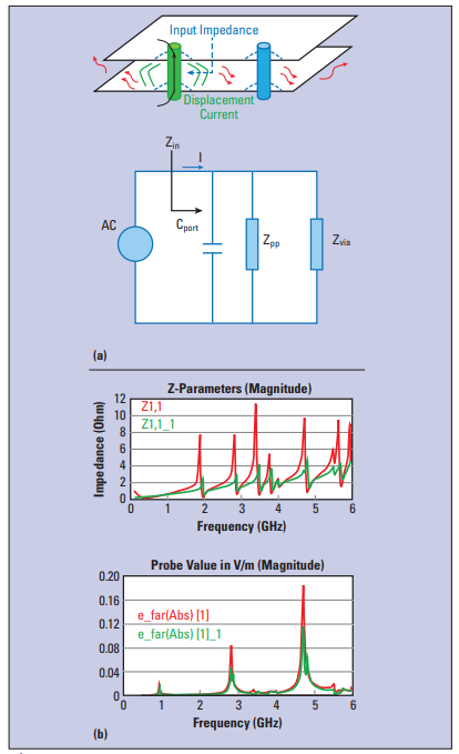
Figure 1. a): GND plane pair and equivalent circuit model, b): input impedance (Zin) and far field amplitude on a sphere 3 m away from the structure.
Blog was published in the SIJ January 2019 Print Issue, Design Tips: Page 44.