
As data rates in high-speed digital systems continue to rise, maintaining signal integrity in connectors like Peripheral Component Interconnect Express (PCIe) becomes increasingly critical. This paper examines the impact of impedance discontinuities introduced by variations in Baseboard and Add-in Card traces, particularly as rise times get faster with each PCIe generation. Using full-wave 3D electromagnetic simulations, various scenarios including changes in pad widths, and connector body impedance are analyzed and validated through measurements. Results demonstrate that impedance discontinuities introduced at the connector mating interface and associated PCB footprints significantly impact return loss performance, while variations in the connector body impedance have comparatively limited influence. These findings provide valuable insights into optimizing PCIe connector designs.
1. Introduction
The growing demand for higher data rates in digital systems has heightened the importance of analyzing interconnects like PCIe connectors to maintain signal integrity. PCIe connectors are among the mainstream interconnects used in high-speed applications, and their performance is critical to the reliability of modern systems. Emerging issues in PCIe connectors, particularly at higher generations like PCIe Gen7, make it essential to investigate how variations in design elements, such as Baseboard and Add-in Card traces and pads, can affect the performance. Changes to Baseboard traces, pad lengths, and widths as well as similar variations associated with the Add-in Cards, can introduce impedance discontinuities. As rise times get faster with the doubling of the Nyquist frequency for each PCIe generation, the impact of these discontinuities becomes more pronounced since PCIe 7.0 specification is planned to deliver another generational leap in performance, targeting a data rate of 128 GT/s, effectively doubling the speed of the PCIe 6.0 specification [1]. These disruptions in signal integrity can lead to significant challenges in ensuring reliable performance in high-speed environments.
While both insertion loss (IL) and return loss (RL) are key signal integrity metrics, they represent different physical phenomena. IL quantifies the amount of signal energy transmitted through an interconnect, whereas RL measures the portion of the signal reflected due to impedance discontinuities. In high-speed PCIe interconnects, reflections are often strongly influenced by impedance variations occurring at the connector mating interface and the associated PCB footprints, where traces transition into pads and connector contacts.
This study investigates how impedance variations at these interface regions influence RL performance in PCIe connectors. Using full-wave electromagnetic models built in CST Studio Suite®, a registered trademark of Dassault Systèmes, the investigation is conducted including not just the connectors but also Add-in Card and Baseboard pads representing realistic scenarios.
The results demonstrate that impedance discontinuities associated with the mating interface and PCB footprints can have a significantly greater impact on RL than variations occurring within the connector body itself. These findings highlight the importance of carefully controlling footprint geometry and trace-to-pad transitions when integrating high-speed connectors into system channels.
2. Problem Statement
Mitigating return loss (RL) failures in high-speed serial links presents unique challenges compared to addressing insertion loss (IL) issues. Return loss arises from the cumulative reflections produced by impedance discontinuities along the transmission path. While all discontinuities contribute to the overall reflection behavior, impedance variations occurring near the transmitter or receiver can have a stronger influence on the measured RL because the resulting reflections experience minimal propagation attenuation before reaching the reference plane.
In high-speed connector systems such as PCIe, many of these critical discontinuities occur at the connector mating interface and the associated PCB footprints, where traces transition into pads and connector contacts. Variations in pad geometry, trace-to-pad transitions, and local material properties can therefore significantly influence RL performance, even when the connector body impedance itself remains relatively well controlled.
This paper investigates how such interface-related impedance variations influence RL in PCIe connectors by analyzing changes in pad widths, connector body dielectric properties, and footprint geometries. The analysis compares the impact of discontinuities located near the mating interface with those occurring within the connector body. The results highlight the sensitivity of RL to impedance variations at the connector interface and PCB footprint, providing practical guidance for system integrators designing high-speed interconnect channels.
3. Simulation Setup for Proposed Analysis
PCIe channels are typically designed with a differential impedance target of 85 Ω ±10%, which includes the combined impedance contribution of PCB traces, connector transitions, and vias. While the connector itself is designed to approximate an 85-Ω differential impedance, the traces on the Baseboard and Add-In Card are designed as ~42.5 Ω single-ended transmission lines, resulting in an 85 Ω differential impedance when routed as a differential pair. Maintaining impedance continuity across traces, pads, vias, and connector interfaces is critical to minimizing reflections and ensuring compliance with PCIe return loss specifications.
For the proposed investigation of PCIe connector performance, a test setup with the following components is considered:
- Baseboard Trace: 50mils in length.
- Baseboard Pad: The pad where the connector is mounted on the Baseboard.
- Connector: The primary focus of the performance evaluation.
- Add-in Card Plug Pad: The pad on the Add-in Card where the connector interfaces.
- Add-in Card Trace: 50mils in length.
A. Simulation Process
The simulation process involves importing the Add-in Card footprint, connector, and Baseboard footprint into a 3D electromagnetic solver, CST Studio Suite®. Material properties, boundary conditions, and mesh properties are then defined in the software. Single-ended ports are established at the ends of the traces on both the Add-in Card and Baseboard, serving as reference planes for calculating Scattering parameters (S-parameters).
Figure 1 provides a detailed illustration of the design, highlighting how the connector integrates with the Add-in Card and Baseboard emphasizing trace-to-pad transitions and reference planes [2].
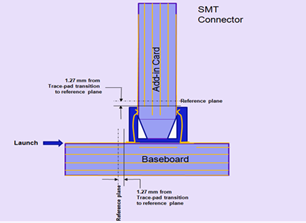
Fig. 1. Illustrates the physical layout and geometry of an SMT (Surface Mount Technology) PCIe connector interfacing between an Add-In Card and a Baseboard.
B. Port setup and signal excitation
Figure 2 illustrates the port setup on the Add-in Card side. To ensure accurate signal excitation, wave ports are applied to the coaxial structures at the ends of the traces.
- The bent connector pins represent the portion of the connector that mates with the Add-in Card pad, ensuring proper electrical continuity [3].
- On the Baseboard side, the connector terminates at a similar port setup, completing the 3D full-wave simulation environment.
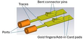
Fig. 2. 3D model showing port setup on Add-in Card side with traces, mated connector pins and pads.
C. Full wave simulation and sparameter analysis
This study utilizes full-wave 3D electromagnetic simulations to generate S-parameter models. These models were solved up to 32 GHz with 10 MHz steps, ensuring high accuracy for evaluating critical signal integrity parameters such as impedance profiles, IL and RL. These S-parameters are essential for understanding the connector's behavior in high-speed PCIe applications. The model and analysis methodology follow the guidelines outlined in the PCIe specifications, ensuring that the results are aligned with industry standards.
D. High Speed PCB material considerations
Since the analysis focuses on high-speed PCIe connectors, the printed circuit board (PCB) material used in the simulations was Megtron-6, which is commonly used in high-speed platforms due to its low dielectric loss characteristics. The dielectric properties were modeled using the Dj-Sarkar model to capture frequency-dependent behavior of the substrate. The dielectric constant was specified as Dk = 3.4 at 10 GHz, with a loss tangent Df = 0.002 at 10 GHz. The signal layers were modeled using 35 μm copper thickness (1 oz copper) and copper conductivity was assumed to be 5.6 × 10⁷ S/m. For simplicity, the simulations assumed rectangular trace cross-sections and etch trapezoidity and surface roughness effects were not included.
E. Port configuration and impedance matching
In the simulations, each signal pin is treated as part of a port pair, with ports placed at both ends of the trace, and ports are configured as single-ended. Ground pins are typically connected by a conducting structure such as a plane or slab of metal, which provides a perfect reference at the port signals [4].
The simulations assume a reference impedance of 50 Ω at the ports. Post-simulation, the S-parameters are renormalized to match the connector's target impedance using a process involving conversion to Z- or Y-parameters, impedance adjustment, and reconversion to S-parameters [5]. For PCIe connectors, the standard impedance is 85 Ω, and this is reflected in the impedance profile results.
4. Discontinuity Analysis and Novel Observations
In this section, details of various analysis for discontinuities near and away from the endpoints of the connector is given.
- Variations in Connector Body Impedance
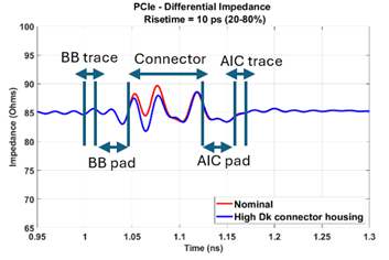
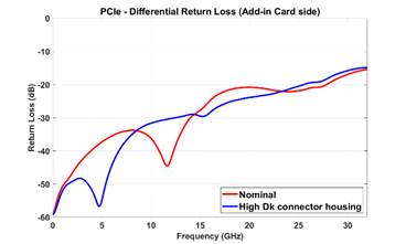
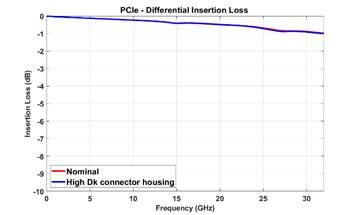
To study the impact of connector’s central body impedance, the dielectric constant of the housing was increased, introducing a capacitive discontinuity. Figure 3(a) highlights the differential impedance variation localized in the connector’s central region, which minimally impacts RL and IL, as shown in Figure 3(b, c) and 3(d) respectively. In the impedance plot, markers identifying the different sections of the simulated structure (baseboard trace and pad, connector, and add-in card trace and pad) have also been added to clearly indicate the physical regions corresponding to the observed impedance variations. It is worth noting that discontinuities closer to the reference plane contribute more strongly to the measured return loss. In practical PCIe systems, however, the effective reference planes are typically located farther from the connector than in the evaluation structure used here, which may further reduce the system-level impact of these localized impedance variations.
To quantify this variation, the nominal Dielectric constant (Dk) value used was 3.1. Initially, Dk values of 3.2 and 3.3 were tested, but these only resulted in a 2-ohm impedance deviation, which was insufficient to significantly affect return loss. Therefore, a higher Dk value of 3.4 was chosen, introducing an impedance discontinuity of 3-5 ohms in the center of the impedance profile to introduce any noticeable return loss change. The loss tangent (Df) was kept constant to isolate the effect of Dk variations.
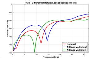
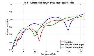
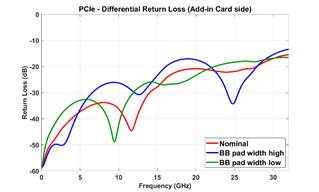
- Variations in Pad Widths on Add-in Card/Baseboard Sides
Pad width variations on both the Add-in Card and Baseboard sides were analyzed to assess their impact on impedance, RL and
IL. Three scenarios were considered for each side:
- Nominal pad width (reference case).
- Increased pad width, introducing capacitive discontinuity.
- Reduced pad width, causing an inductive discontinuity.
(a)
(b)
(c)
(d)
Fig. 3. Impedance, RL and IL Profiles for changes in connector body parameters: (a) impedance (b, c) RL and (d) IL.
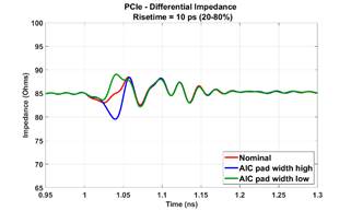
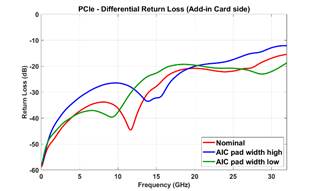
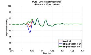
Figures 4(a) and 5(a) illustrate the impedance profiles for the Add-in Card and Baseboard pad width variations, respectively. For both cases, the nominal scenario serves as the baseline, where increased pad width introduces capacitive discontinuities, and reduced pad width results in inductive discontinuities.
For the Add-in Card, the nominal pad width was 0.55 mm. Initially, variations of 0.50 mm (lower) and 0.60 mm (higher) were considered, but these only resulted in a 2-ohm impedance deviation, which had minimal impact on return loss. To induce more noticeable effects, an extreme case of 0.45 mm (lower) and 0.65 mm (higher) pad width was selected, leading to a 3-5 ohm impedance deviation, as seen in Figure 4(a). Similarly, for the Baseboard, the nominal pad width was 0.53 mm, with variations of 0.48 mm (lower) and 0.58 mm (higher), producing a similar 3-5 ohm impedance deviation, as shown in Figure 5(a).
The return loss (RL) results, shown in Figures 4(b, c) and 5(b, c), highlight significant sensitivity to pad width changes. Figure 4(b) presents return loss observed from one side of the interconnect, while Figure 4(c) shows return loss from the opposite side. A similar trend is observed in Figures 5(b) and 5(c), where return loss from both perspectives reinforces the impact of pad width variations.
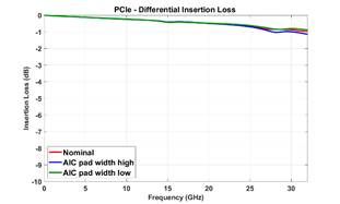
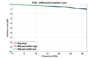
As seen in Figures 4(b, c) and 5(b, c), return loss deviates by 5-10 dB at multiple frequency points due to impedance discontinuities caused by pad width variations, leading to increased reflections that directly impact signal integrity. In contrast, the insertion loss (IL) plots in Figures 4(d) and 5(d) show minimal variation, with changes remaining below 0.5 dB across most of the frequency range. This suggests that insertion loss is relatively unaffected by the discontinuities under investigation. Given the pronounced impact on return loss, it becomes the primary concern for ensuring optimal signal transmission in this PCIe structure.
To ensure a fair comparison between pad width variations and connector body impedance changes, the impedance deviation of 3-5 ohms induced by pad width variations was kept consistent with the impedance deviation introduced by the central body impedance changes discussed in Section IV(A). Since we have already established that insertion loss remains largely unaffected in both cases, we do not present insertion loss results in the subsequent section on validation through measurements, as the primary verification focuses on the impact of discontinuities on return loss performance. Additionally, since the simulated return loss results from both sides show close agreement, the measurement results will present return loss data from only one side for brevity.
C. Theoretical Explanation
The observed difference in return loss sensitivity to discontinuity locations can be explained using fundamental transmission line theory. The reflection coefficient for a single impedance discontinuity is given by [6]:
![]() (1)
(1)
(a)
(b)
(c)
(d)
Fig. 4. (a) Impedance profile, (b, c) RL and (d) IL results for Add-in Card pad width variations.
(a)
(b)
(c)
(d)
Fig. 5. (a) Impedance profile, (b, c) RL and (d) IL results for Baseboard pad width variations.
The corresponding return loss is defined as
RL = -20 log₁₀ |Γ| (2)
In practical interconnect structures, the reflection observed at the measurement port depends not only on the magnitude of the local impedance discontinuity but also on its distance from the reference plane. Discontinuities located close to the transmitter or receiver produce reflections that reach the measurement port with minimal propagation attenuation. In contrast, reflections generated by discontinuities located farther along the transmission path must travel a longer distance before reaching the measurement plane. During this propagation, the reflected signal experiences attenuation due to conductor and dielectric losses present in high-speed channels. Consequently, reflections originating from distant discontinuities contribute less to the measured return loss than identical discontinuities located near the endpoints of the interconnect.
D. Validation through Measurements
To further validate the findings of this study, two distinct measurement scenarios were analyzed. The measurements were conducted up to 50 GHz with a frequency step size of 10 MHz using a Vector Network Analyzer (VNA). De-embedding was performed up to 32 GHz using a 2X thru calibration method, which significantly simplifies the de-embedding procedures while maintaining excellent correlation in IL, RL, NEXT, and FEXT over the full frequency range of measurement [6].
However, traditional methods like through-reflect-line (TRL) present challenges, as they require using the same fixture in the calibration kits and the device under test (DUT), which is difficult to achieve in practice due to manufacturing nonidealities. To address this, we used an impedance-corrected 2x-thru de-embedding method, which implements a peeling process to remove errors caused by differences between the Fixture-DUT-Fixture and reference 2x-thru impedance. This approach is inherently more robust, as fixture manufacturing tolerances do not impact the de-embedding results, and it improves calibration accuracy by partially correcting fixture mismatches [7], [8].
The measurement data in this paper was de-embedded using the In-Situ De-embedding (ISD) method. In-Situ De-embedding (ISD) is designed to address non-causality issues in device-under-test (DUT) results by using a simple 2x thru test coupon and numerical optimization. This approach ensures causal DUT results, enhances de-embedding accuracy [9].
Differential impedance results have been obtained from the VNA data by performing an Inverse Fast Fourier Transform (IFFT) of the frequency-domain S-parameter data. This approach enables the extraction of time-domain impedance characteristics, allowing for a more comprehensive analysis of discontinuities and their impact on signal integrity.
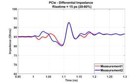
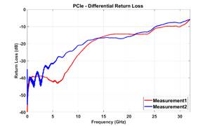
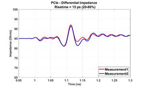
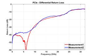
Scenario 1: Trace and Pad Width Variations
In this scenario, the trace and pad widths in the measurement results were different but connector impedance was same. The objective was to evaluate the impact of changes in trace and pad dimensions on RL performance. Figures 6(a) and 6(b) illustrate the impedance or time domain results and RL profile for this case, highlighting significant change in RL loss performance under 14 GHz.
(a)
(b)
Fig. 6. Measured Impedance and RL Profile for Trace and Pad Dimension Variations: (a) Measured impedance profile, and (b) measured RL profile.
Scenario 2: Connector Impedance Variation
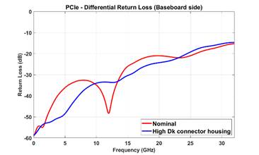
In this case, the trace and pad impedance showed minimal variation, while the connector impedance exhibited differences between 1.12 ns and 1.17 ns, as illustrated in Figure 7(a). Despite the variations in connector impedance, the RL results shown in Figure 7(b) indicate no substantial change in performance.
The results demonstrate that variations in trace and pad widths significantly influence RL performance, even when connector impedance remains unchanged. Conversely, changes in connector impedance have a minimal impact on RL when trace and pad impedance are constant. These findings align with the Discontinuity Proximity Effect, emphasizing that discontinuities closer to the endpoints of a transmission line have a greater impact on RL compared to those occurring in the central region.
(a)
(b)
Fig. 7. Measured Impedance and RL Profile for Connector Impedance Variations: (a) Measured impedance profile, and (b) measured RL profile.
To quantify the variations beyond traditional frequency-domain return loss plots, a metric called Integrated Return Loss (IRL) has been utilized. IRL provides a single numerical value representing the overall return loss across a frequency range, allowing for easier comparison between different scenarios.
The iRL results in Table I confirm that impedance discontinuities near transmission line endpoints have a more significant impact on return loss. Scenario 1 exhibits a nearly 6% change, while Scenario 2 shows only 3%, reinforcing the Discontinuity Proximity Effect.
Table I: Integrated Return Loss (IRL) and Percentage Change for Different Scenarios
Scenario |
Case |
Integrated Return Loss (dB) |
Percentage Change (%) |
Scenario 1 |
Case 1 |
-32.24 |
— |
Scenario 1 |
Case 2 |
-30.33 |
-5.92% |
Scenario 2 |
Case 1 |
-34.53 |
— |
Scenario 2 |
Case 2 |
-33.52 |
-2.92% |
CONCLUSION
The study shows that impedance variations at the connector mating interface and PCB footprints significantly influence return loss performance, whereas variations within the connector body have comparatively smaller impact. These findings highlight the importance of careful footprint and pad design when integrating PCIe connectors into high-speed channels.
ACKNOWLEDGEMENT
The simulation models and measurement data used in this study are based on proprietary PCIe® CEM connector designs developed by Amphenol Communications Solutions.
REFERENCES
[1] A. Wander, "Navigating Signal Integrity Challenges: Transitioning from PCIe Gen6 to Gen7," Signal Integrity Journal, Feb. 2024. [Online]. Available: https://www.signalintegrityjournal.com/articles/3462-navigating-signal-integrity-challenges-transitioning-from-pcie-gen6-to-gen7.
[2] Y. Li, Y. Huang, A. S. Wander, A. Key, L. He, S. B. Smith, and Y. Zhou, "PCIe Gen. 5 CEM Connector and Add-In Card PCB Design Optimizations," in 2019 DesignCon, Santa Clara, CA, USA, Jan. 2019.
[3] C. Li, K. Cai, M. Mousavi, M. K. Mathew, B. Sen and D. B. Kim, "Simplified Equivalent Golden Finger Port Setup for Fast and Accurate High-Speed Channel Simulation," 2023 IEEE Symposium on Electromagnetic Compatibility & Signal/Power Integrity (EMC+SIPI), Grand Rapids, MI, USA, 2023, pp. 301-305, doi: 10.1109/EMCSIPI50001.2023.10241699.
[4] S. B. Smith, K. Patel, J. Cin, S. S. Agili and J. Walden, "Effects of High-Speed Signals on Power Integrity," 2018 IEEE Holm Conference on Electrical Contacts, Albuquerque, NM, USA, 2018, pp. 278-285, doi: 10.1109/HOLM.2018.8611677.
[5] D. M. Pozar, Microwave Engineering, 4th ed., Wiley, 2011 , New York, New York.
[6] S. -J. Moon, X. Ye and R. Smith, "Comparison of TRL calibration vs. 2x thru de-embedding methods," 2015 IEEE Symposium on Electromagnetic Compatibility and Signal Integrity, Santa Clara, CA, USA, 2015, pp. 176-180, doi: 10.1109/EMCSI.2015.7107681.
[7] J. J. Ellison and S. S. Agili, "Impedance Corrected De-Embedding," in IEEE Electromagnetic Compatibility Magazine, vol. 11, no. 3, pp. 45-48, 3rd Quarter 2022, doi: 10.1109/MEMC.2022.9982534.
[8] C. -C. Chou and J. -H. Hsu, "An Impedance-Corrected 2x-Thru Calibration," in IEEE Microwave and Wireless Technology Letters, vol. 33, no. 12, pp. 1674-1677, Dec. 2023, doi: 10.1109/LMWT.2023.3325226.