
PCI Express Link is one of the most popular high-speed SerDes designs. It serves wide applications from consumer laptops and desktops to enterprise data servers. As shown in Figure 1, bandwidth provided by PCIE has increased exponentially over time to satisfy industry demands. In the early stage of PCIE Gen1, there was no equalization scheme implemented because of low speeds, and platform signal integrity was the main solution to achieve the specification requirements. TX de-emphasis was adopted for PCIE Gen2 to compensate for the loss of the channel. Then CTLE/DFE (continuous time linear equalizer / decision feedback equalizer) was introduced in the PCIE Gen3 specification to address further channel degradation. PCIE has successfully responded to customer demand over time and currently, the PCIE Gen6 specification is under development with PAM4 signaling to meet a 64Gbps data rate using heavy equalization schemes.

Conventional signal integrity analysis has mainly focused on the signal quality of a given channel in terms of insertion loss, reflection loss, crosstalk noise, and pulse response inter-symbol interference. However, there has been a significant paradigm shift to include the analysis of reliable equalization schemes since no signal integrity analysis is possible on an unequalized waveform where the input signal of a receiver only shows 20~30mV peak-to-peak (p2p) swing that is barely above the noise. Thus, modeling equalization circuit characteristics is extremely important to ensure the success of the final platform implementation and provide a strong signal integrity design guide. In the future, the complexity of circuit implementation will increase dramatically and modeling of high-speed SerDes systems will continue to be a huge challenge.
Interpreted computer languages and graphical block diagram environments are popular tools for modeling SerDes systems because they provide simple and intuitive paths to express the complex concepts needed to represent high-speed wired communication systems. Elaborate models with tens of thousands of lines of code or block diagram models with thousands of elements spread over a dozen abstraction layers are not uncommon.
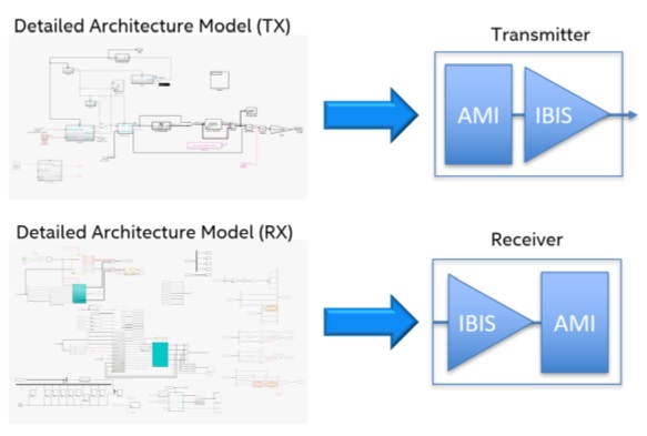
It is also unfortunately common to totally redesign the detailed architectural model to provide an IBIS-AMI model to an anxious customer who is attempting to incorporate the chip into their server system design. This IBIS-AMI model is inevitably late, poorly correlated, and lacking in features needed for complete system-level analysis.
In this paper we first review the common challenges of converting an existing detailed architectural model to an IBIS-AMI model and some of the ways that we have addressed these challenges. This is followed by an illustration of the workflow to model Intel’s 56G PAM4 SerDes.
Download the PDF to read the entire paper.
This paper was originally presented at DesignCon 2020.