
What Happens When the Die Model is Incorrect?
As voltage margins for power rails continue to decrease, end-to-end power integrity modeling is already difficult without having to be concerned if all of your simulation models are correct. As system designers, we typically assume that all of the vendor models are correct.
So, what does an engineer do if one of the ASIC die models needed for a power integrity simulation is incorrect?
When the die model is incorrect, timing jitter and voltage ripple are affected. In the example shown by Figure 1, a 51% decrease in the voltage ripple occurs, and a 30% decrease in jitter occurs just by increasing Cdie from 3.29 nF to 6.49 nF. Figure 1 shows that the voltage ripple is failing the specification for this power domain at 3.29 nF.
 Figure 1. Voltage ripple and timing jitter response with two different Cdie values.
PDN Impedance Impact From the Die Model
As previously shown, when the die model is incorrect, both timing jitter and voltage ripple are impacted. Figure 2 provides an example of a system that includes an ASIC die with the package, the printed circuit board, and a power supply, also referred to as a voltage regulator module. Each of these components has an interconnect and parasitics that make up the power distribution network (PDN) that delivers power from the power supply to the ASIC die load.
 Figure 2. System model with ASIC die.
The ASIC die load model drives the target impedance requirements of the system PDN. The passive portion of an ASIC die model consists of parasitic Cdie and Rdie. Cdie is the on-die decoupling capacitance attached to the resistive grid on the die. Rdie will be the function of the metal power grid on the die and the resistance of the bumps and any on-die capacitors.1 Figure 3 shows an impedance vs. frequency plot of an example die model, not including the rest of the PDN. This example illustrates where the die model begins to impact the PDN of a system.
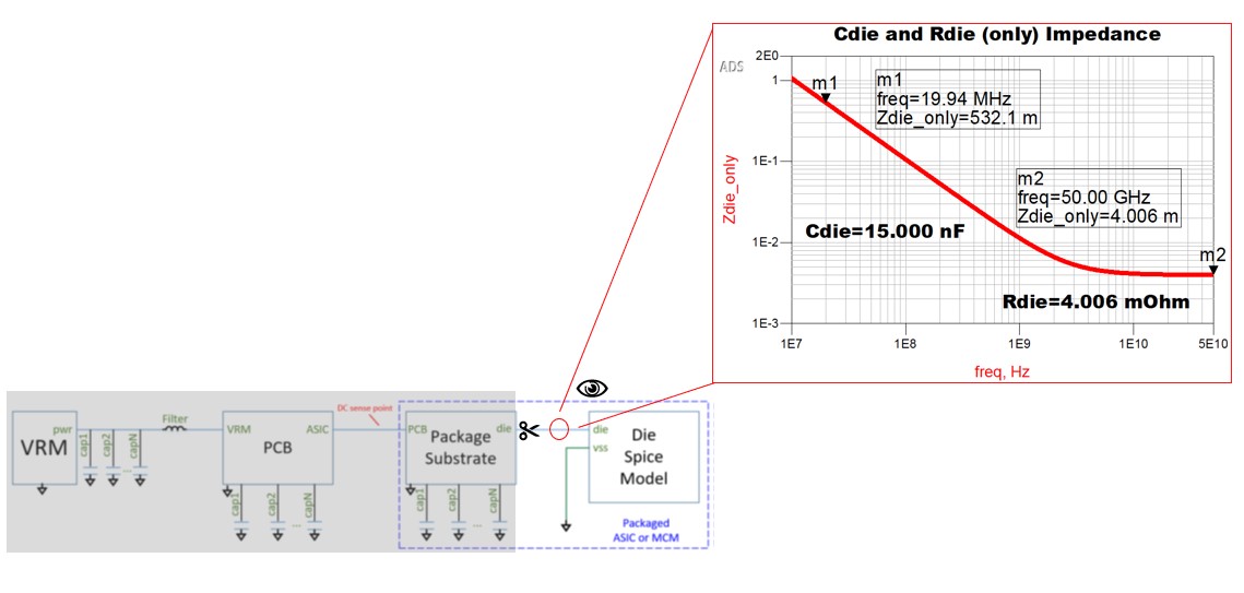 Figure 3. PDN impedance impact from die model.
Figures 4 and 5 augment the example to help understand the importance of the PDN effects of the die model with the package. Figure 4 is an example of a die model and a package without package capacitors included, and Figure 5 is an example of the same die model and package with the on-package capacitors included. When comparing the impedance shown in Figures 4 and 5, the inductance between the package and the ASIC die dominates this part of the PDN. This is driven by the package inductance (Lpkg), which changes from 12pH without package capacitors included and 6pH with package capacitors included.
Notice in Figure 5 that by adding (43) 10 nF on-package capacitors, very little change is observed in the impedance response regardless of whether Lpkg is equal to 6 pH or 12 pH. This implies the inductance between the die and the package limits the effectiveness of the capacitors located on the package.
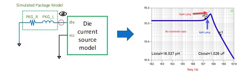 Figure 4. Package-die impedance curve without package substrate capacitors.
 Figure 5. Package-die impedance curve including package substrate capacitors.
Why Should We Care About the Die Model?
Four simple package and die model configurations are shown in Figures 6, 7, 8, and 9. In these four examples, a 100 mA, 1 ns risetime, and 10 ns wide pulse are applied to the PDN at the die. The voltage responses are shown by varying the on-package capacitance and the on-die capacitance.
When comparing Figure 6 to Figure 7, notice (when Cdie is 1 nF) by adding an almost unlimited amount of capacitance to the package, the voltage ripple at the die does not significantly change. Again, this emphasizes that the inductance between the package and the ASIC die limits on-package capacitance effectiveness.
In contrast, comparing Figure 6 to Figure 8 (where Cdie is increased to 5 nF), the voltage ripple at the die is reduced by 55%.
Also, comparing Figure 6 to Figure 9 (where Cdie is increased to 10 nF), the voltage ripple at the die is reduced at the die by 74%. This emphasizes two things: inductance between the package and die limits the on-package capacitor's high-frequency effectiveness and the importance of Cdie on the voltage ripple at higher frequencies seen by the die.
 Figure 6. PDN impedance and step load response with Cdie=1 nF, Cpkg=8 uF.
 Figure 7. PDN impedance and step load response with Cdie=1 nF, Cpkg=100 mF.
 Figure 8. PDN impedance and step load response with Cdie=5 nF, Cpkg=8 uF.
 Figure 9. PDN impedance and step load response with Cdie=10 nF, Cpkg=8 uF.
Power Integrity Case Study
The specifications given by an IP vendor for the DDR PHY integrated on this ASIC are the following:
- 30 mV ripple (> Fclk)
- 150 mV ripple (< Fclk)
The DDR4 PHY die model provided by the IP vendor had the following specifications:
- Cdie = 3.29 nF
- Rdie = 4.23 mΩ
How Do You Know if the Die Model from a Vendor is Correct?
When the DDR PHY IP vendor initially provided the die model specifications, it appeared to have insufficient on-die capacitance for an x72 memory controller. To help make this case, another Cdie model for a memory supplier x16 SDRAM was initially used to compare to the Cdie on this DDR PHY. Figure 10 shows an example IBIS Quality report from a memory supplier, which details the amount of on-die capacitance. As shown in Figure 10, the x16 SDRAM has more than double the amount of on-die capacitance than the x72 DDR PHY memory controller, further raising suspicion that this DDR PHY Cdie value is incorrect.
 Figure 10. Depiction of IBIS Quality Report from Micron.2
DDR is a parallel bus where multiple nets are driven simultaneously, causing simultaneous switching output noise on the power nets. Another way to examine Cdie for a DDR application is to examine the amount of capacitance per DQ/DQS/DM. Comparing the per DQ/DQS/DM die capacitance from the memory vendor in Figure 10 at 352 pF to Figure 11 from the DDR PHY IP vendor at 33.23 pF, notice the significant 10x difference between the two. Again, this raises suspicion of the Cdie value provided for the DDR PHY from the IP vendor.
 Figure 11. Initial vendor DDR PHY Cdie model.
A schematic encompassing the full PDN impedance is shown in Figure 12, and the results are plotted in Figure 13 after optimizing the on-package capacitors with Cdie = 3.29 nF. Notice the worst impedance peak occurs at 527 MHz, as indicated by marker m4. The goal of the simulation in the time domain is to create a stimulus as close to this impedance peak, causing a worst-case scenario to test the robustness of the PDN. However, since the data rate is 2400 MT/s, the closest period to 527 MHz is either 480 MHz or 600 MHz. Figure 13 shows the impedance of the PDN is slightly higher at 480 MHz versus 600 MHz. Thus, a 480 MHz test pattern will be used to create the worst-case PDN stimulus.
 Figure 12. VDDQ PDN impedance simulation setup.
  Figure 13. VDDQ PDN impedance from ASIC die with Cdie = 3.29 nF.
Using the circuit shown in Figure 14, a 5-bit repeating “11100” bit pattern will provide a 480 MHz period to ensure the worst-case excitation is used during simulation.
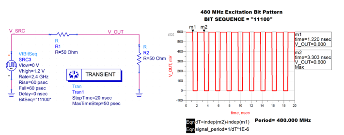 Figure 14. Depiction of 480 MHz excitation test bit pattern.
Figure 15 is a schematic for a DDR4-2400 read simulation. This schematic uses the DDR4 PHY IBIS model connected to the PDN shown in Figure 12. Each DDR4 memory chip is also connected to the PDN shown in Figure 12 and includes the SDRAM PI die model.
To ensure adequate loading, all signal nets are included in the simulation, which includes DQ[71:0], DQS_c/t[8:0], CK0_c/t[0], A[13:0], WE_n, CAS, RAS, ACT_n, ODT, PARITY, BA[1:0], BG[1:0], and CS0_n. All the data nets are set to 48 Ω drive strength at each SDRAM, connected to the memory controller through 48 Ω transmission lines, and terminated at the memory controller with the On Die Termination (ODT) set to 48 Ω. All the Command-Address-Control (CAC) nets are connected from the memory controller to all nine SDRAMs through a fly-by topology using 48 Ω transmission lines. The memory controller is set to 48 Ω drive strength.
All the IBIS models are set to the MAX corner to ensure the worst-case current is used with the 480 MHz excitation data pattern. Figure 16 represents the eye diagram of DQ0 after running the simulation. All data and CAC signals had wide-open eyes like the eye shown in Figure 16.
 Figure 15. DDR4-2400 READ simulation setup to assess VDDQ compliance.
 Figure 16. Depiction of DQ0 eye diagram result for DDR4-2400 READ.
The DDR4 PHY IP vendor specified the voltage ripple requirement as 150 mV peak-to-peak when less than Fclk, where Fclk is 1.2 GHz, and 30 mV peak-to-peak when greater than Fclk. Figure 17 shows the VDDQ voltage response at the ASIC die on the package for a DDR4-2400 read simulation with all IBIS corners set to MAX and represents the worst-case scenario for simulation. The plot on the left represents the sense-corrected VDDQ voltage response and shows a peak-to-peak voltage ripple of 92 mV. The plot on the right is a high-pass filtered VDDQ voltage response when the cutoff is set to Fclk. As shown by the right plot, the high-frequency voltage ripple spec is 60 mV peak-to-peak and is more than double the specification limit. This implies that Cdie is not large enough for this DDR4 PHY.
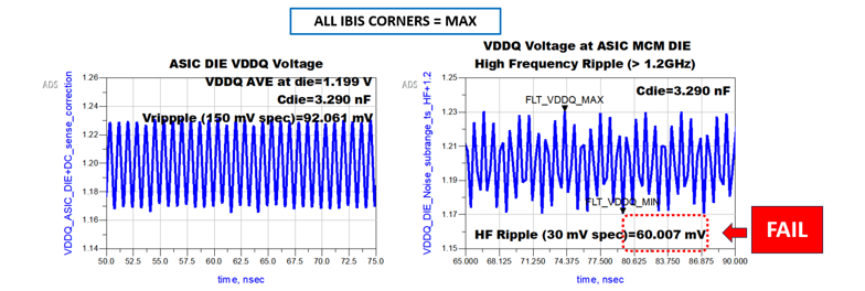 Figure 17. VDDQ voltage response at ASIC DIE, with Cdie = 3.29nF.
How to Determine the Minimum Cdie Value
It is important first to understand the ASIC power domain's transient current to verify if the die model is accurate or has enough on-die capacitance to manage the high-frequency currents. This transient current is what ASIC designers refer to as battery currents and is the raw, unfiltered current. In other words, this current is what the ASIC is demanding before Cdie and Rdie are included. Using the simulation model shown in Figure 15, the raw transient current is plotted in Figure 18. Using Equation (1), the ∆I current can be determined, where 4/π comes from the Fourier Transform of a square wave.3 As previously discussed, the high-frequency voltage ripple specification which the ASIC designer provides is 30mV. With reference to Equation (2), ZTGT(min) can be determined and then used in Equation (3) to determine the minimum Cdie, and shows the minimum Cdie must be greater than 6.19 nF. This indicates that 3.29 nF is insufficient to meet this IP vendor's voltage ripple requirements.
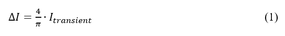
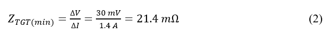

 Figure 18. RAW die VDDQ current, no passives.
Using this information, the IP vendor later confirmed they gave us an incorrect Cdie value. The correct Cdie value for this DDR4 PHY is 6.49 nF at the worst-case corner, which is very close the calculated 6.19 nF minimum found using Equation (3).
Using the updated Cdie value, the full PDN impedance is replotted below in Figure 19. Notice the worst impedance peak now occurs at approximately 300 MHz, as indicated by marker m1.
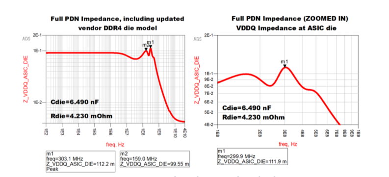 Figure 19. VDDQ PDN impedance from ASIC die with Cdie = 6.49nF.
Using the circuit shown in Figure 20, it is verified that a “1111000” bit pattern will provide a 300 MHz period to ensure the worst-case excitation is used during simulation.
 Figure 20. Depiction of 300 MHz excitation test bit pattern.
Figure 21 is the updated VDDQ voltage response at the ASIC die on the package when Cdie is 6.49 nF. The plot on the left represents the sense-corrected VDDQ voltage and shows a peak-to-peak voltage ripple of 67.5 mV, a 26.6% reduction from the previous result in Figure 17. The plot on the right is the high-pass filtered VDDQ voltage response when the cutoff is set to Fclk. As shown by the right plot, the high-frequency voltage ripple spec is 29.50 mV peak-to-peak, which is now passing the specification limit and proves that Cdie is now large enough for this DDR4 PHY.
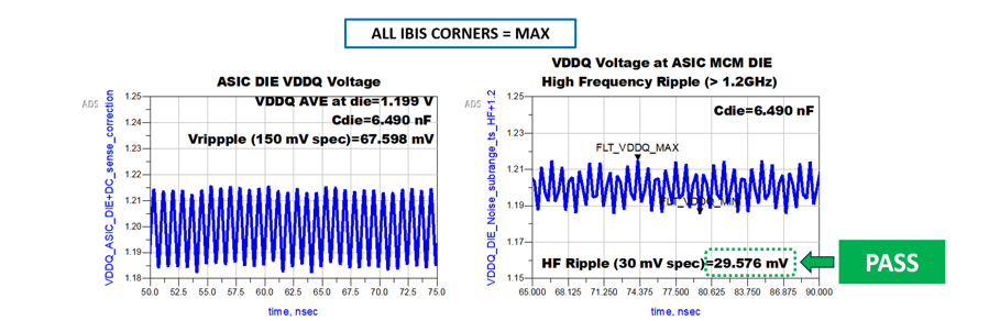 Figure 21. VDDQ Voltage response at ASIC DIE, with Cdie=6.49 nF.
Conclusions
In summary, don’t always trust the models you get from vendors! Supplier models are not always correct. As designers, we need to hold IP suppliers accountable. This means, when integrating IP from a supplier, ask them to confirm what the Cdie value is for each IP power domain, and you should also:
- Ask for a quality report
- Ask for manual calculation for total capacitance on each power domain (C=Dk·ε0·A/D), where:
- The foundry tech file provides the dielectric constant (Dk)
- The MIM cap area (A) or capacitors per layer area is known
- Distance between layers (D) is known
- Total capacitors per power domain is known.
Lastly, the die model impacts both the PDN noise and timing jitter. An accurate model allows verification of both during simulation.
REFERENCES
- B. Dannan, J. Kuszewski et al. "Improved Methodology to Accurately Perform System Level Power Integrity Analysis Including an ASIC Die," DesignCon, 2022.
- MT40AG4SA-062E SDRAM, Micron.
- L.D. Smith, E. Bogatin, Principles of Power Integrity for PDN Design—Simplified: Robust and Cost Effective Design for High Speed Digital Products, Prentice Hall, 2017.
- S. M. Sandler, A. K. Davis, Power Integrity Using ADS, Faraday Press, 2019.
- PathWave ADS, Keysight.
- PathWave ADS Memory Designer, Keysight.