
This article is part three of a three-part series on DDR5 electrical and timing measurement techniques. Please access part one of the series here and part two of the series here.
Introduction
DDR5 System Validation
DDR5, an upgrade from DDR4, aims to address the growing demand for enhanced memory performance in the face of advancing processor technologies with more cores. DDR5 marks significant advancements over its predecessor, with a primary focus on boosting bandwidth. In system-level simulations, DDR5 at higher data rates demonstrates nearly double the effective bandwidth compared to DDR4-3200. This improvement is achieved through data rate increases and architectural enhancements. DDR5 encompasses data rates from 3200 MT/s to 8800 MT/s. A notable feature is the inclusion of a multi-tap decision feedback equalizer in DQ receivers, countering inter-symbol interference (ISI) effects at higher data rates. These developments aim to meet the rising requirements for bandwidth per core in next-generation CPUs.
Test requirements have similarly evolved to ensure electrical and timing margins are met. With DDR5, there is a more distinct separation between device or component (DRAM) and system validation.
| Component | System | |
| Scope | Data sheet, guaranteed by design parameters and proprietary features | As-configured behavior in typical, real-world environments |
| Test Environment | Independent of system architecture. Standard test load, high quality fixtures | 1 or 2 DIMM per channel (DPC), varying ODT, raw cards |
| Results Depend On | Device only | Device, DIMM configurations, channel, training algorithms |
Table 1. Memory Component vs. System Environment Test Considerations.
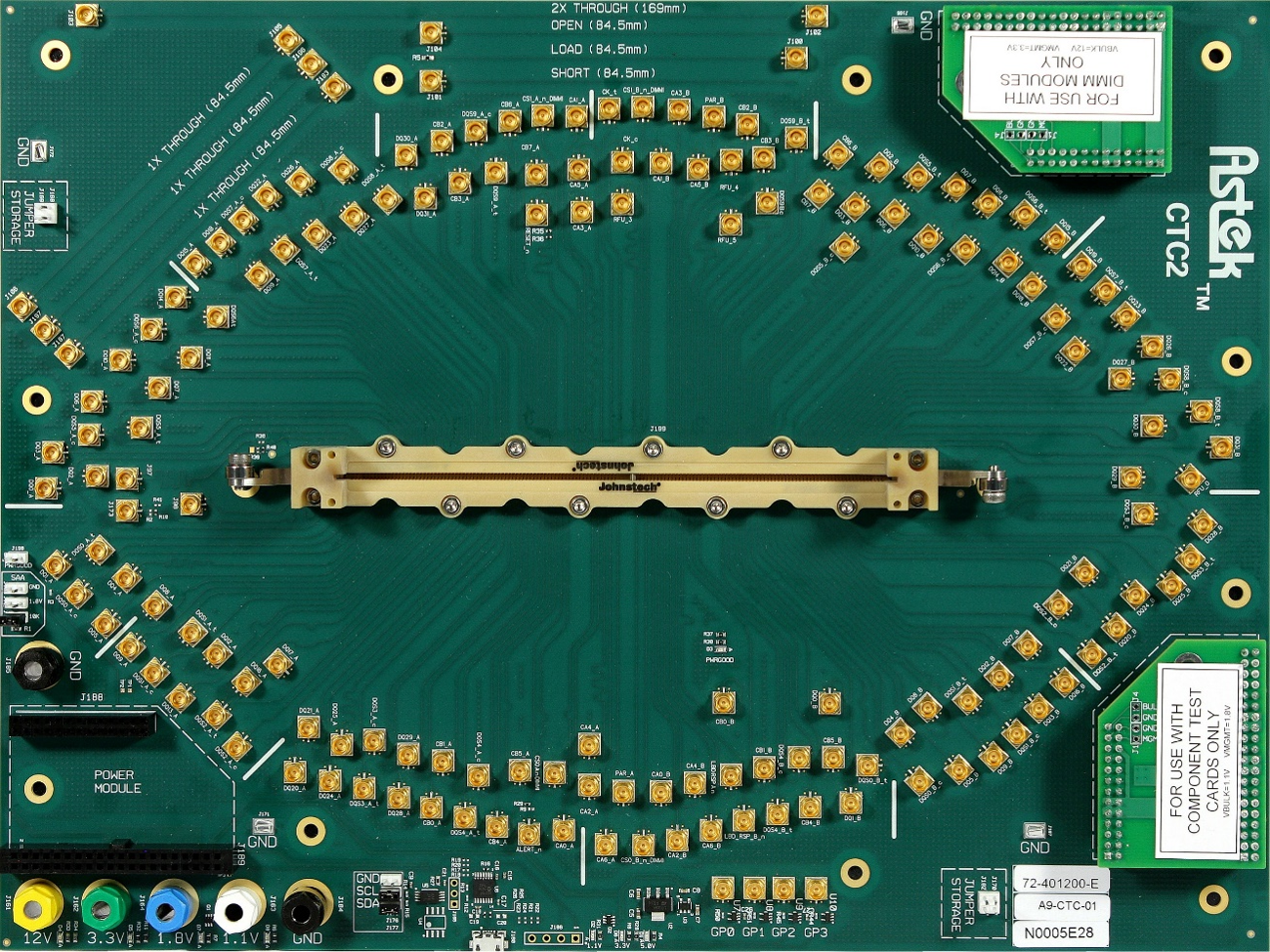 Figure 1.Compliance Test Channel 2 (CTC2) test fixture for component (DRAM, RCD, DB, CKD) and module characterization. (Image courtesy of Astek Corp.)
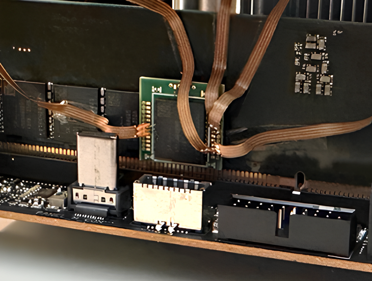 Figure 2. DDR5 BGA interposer with probes attached for system level test.
Signaling Overview
The scope of this article focuses on system level validation where high-speed signals are probed either directly on the system board or with a memory component interposer. Before getting into the various measurement techniques, it is important to understand more about common DDR5 signals. The below table highlights typical signals that should be validated within a system environment to ensure conformance to the JEDEC DDR5 standard.
| Name | Symbol | Type | Comments |
| Clock | CK_t, CK_c | Input | Differential system clock used to latch address and control input signals |
| Chip Select | Cs_n | Input | Active low, single-ended control input used to select multiple ranks and for command qualification |
| Command and Address | CA | Input |
|
| Data | DQ | Input/Output | Bi-directional, single-ended data signals |
| Data Strobe | DQS | Input/Output | Source synchronous differential clock used for latching of read and write operations |
Table 2. Common memory signals.
Test Requirements
DDR5 electrical and timing specifications changed depending on whether the signal is reading or writing data. This means, for example, the slew rate or voltage level depends on the direction and source of the signal. To distinguish the specifications based on signal type test parameters often have prefixes or other designators to reference the data source. In Figure 3, write data is sent from the memory controller (red) and data is read from the memory (blue). Examples of write measurements include “write preamble timing” and “input differential slew rate”. Examples of read measurements are “read high and low output voltage levels”. Because read signaling is only device centric it typically requires a special test load and/or fixture such as the CTC2 for DDR5 (see Figure 1). The burst-dependent nature of DDR5 means the testing must include a burst separation step to analyze a single data capture of bi-directional signaling.
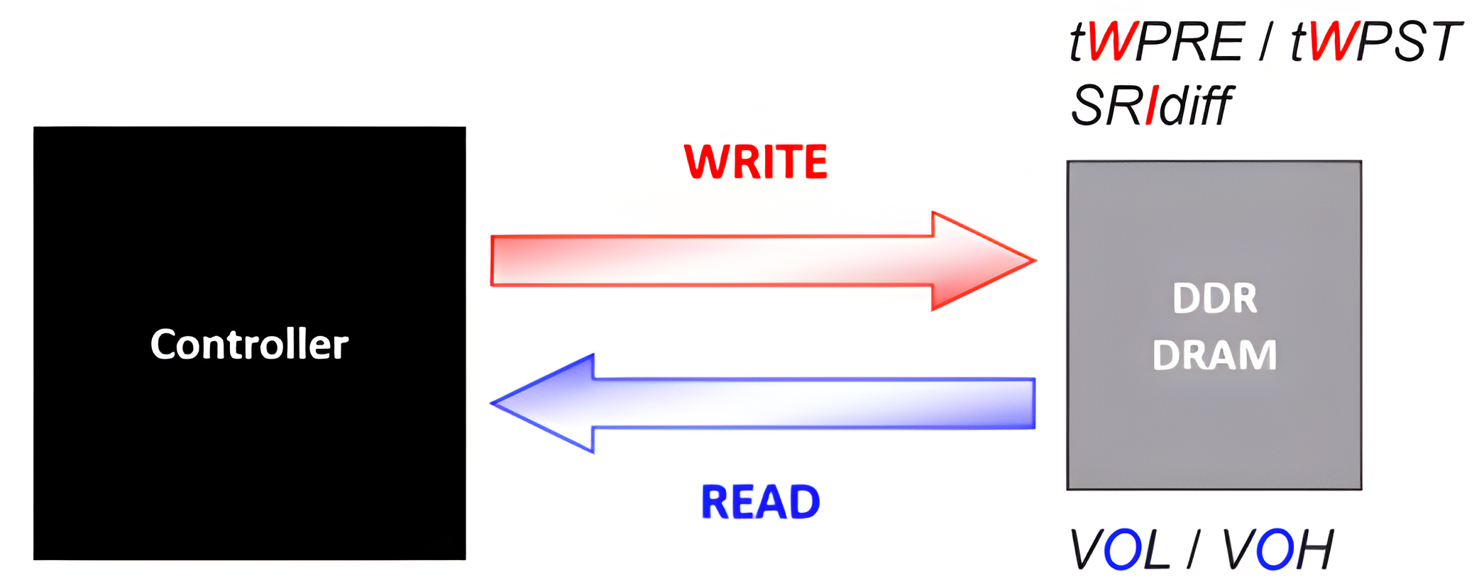
Figure 3. DDR5 parameter names are often defined by direction of signaling.
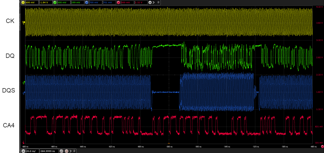 Figure 4. DDR5 clock (CK), data (DQ), strobe (DQS), and Command/Address (CA4) signals.
Burst Separation
Overview
A real-time oscilloscope is the go-to tool for memory electrical validation. It’s high bandwidth, high sample rate capture enables precise timing, jitter, and amplitude measurements. But for a parallel bus with many command and control signals the 4-channel oscilloscope can seem limited in its ability to test the memory interface. So, with a narrow view of the full command bus how exactly is test equipment able to detect read and write bursts? The following are common burst separation techniques used for memory validation.
Phase Relationship
For legacy (DDR4 and earlier) memory systems read and write bursts follow a predictable pattern that makes it easy for test equipment to detect bursts: data is center-aligned with respect to the strobe for writes and edge-aligned for reads. Figure 5 shows an example of DDR4 write data and strobe signals that are center-aligned Much of the burden of timing and skew alignment is placed on the memory controller hence the write data arrives (center-aligned) at the DRAM receiver with minimal skew to make data latching easier. With DDR5, these rules are almost the same except for the writes. To reduce power consumption (DQS clock gating) and ease write training DDR5 uses an unmatched path for the DRAM input. However, there are still other methods that can be used for read and write signaling. Figure 6 shows a variable delay that is possible between write data and strobe signals.
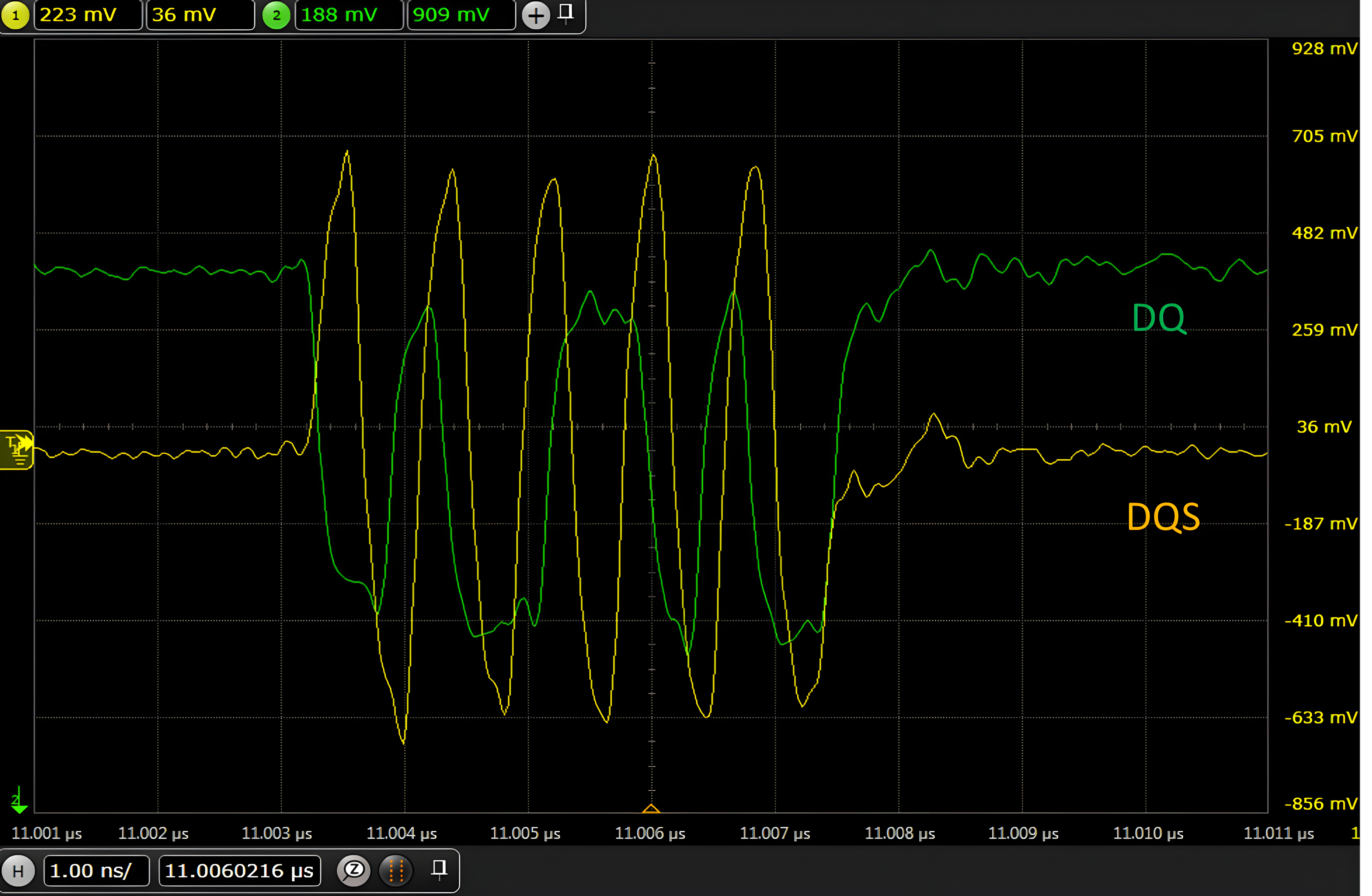 Figure 5. DDR4 write burst showing center aligned DQS to DQ phase relationship.
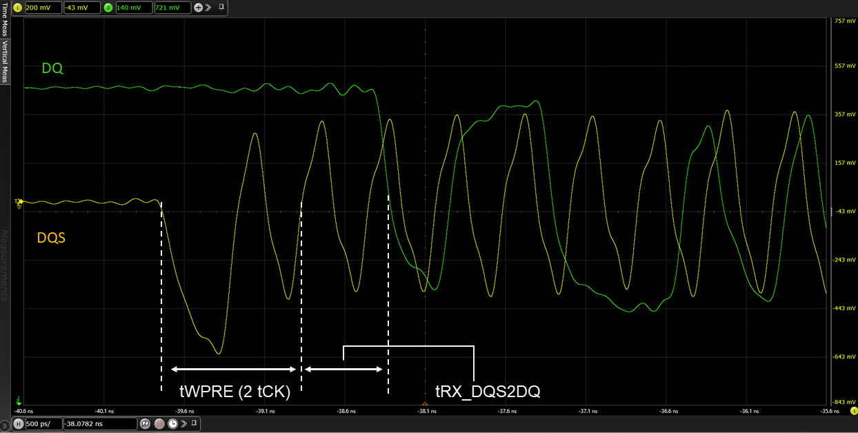 Figure 6. DDR5 write burst showing unmatched delay and phase relationship.
Amplitude Differences
Despite the complex protocol used with DDR5 for storing and retrieving data the higher data rates offer an interesting byproduct to enable burst separation. The higher frequency dependent loss and signal attenuation results in more pronounced amplitude differences between a read and write. Since the memory traffic is captured as close to the DRAM as possible, either directly or with an interposer, the read data is expected to be higher amplitude. Knowing these differences can simplify the burst identification process. Some DDR5 compliance tools offer this feature and can even use machine learning algorithms to better distinguish between a full swing burst and a “peaked” edge.
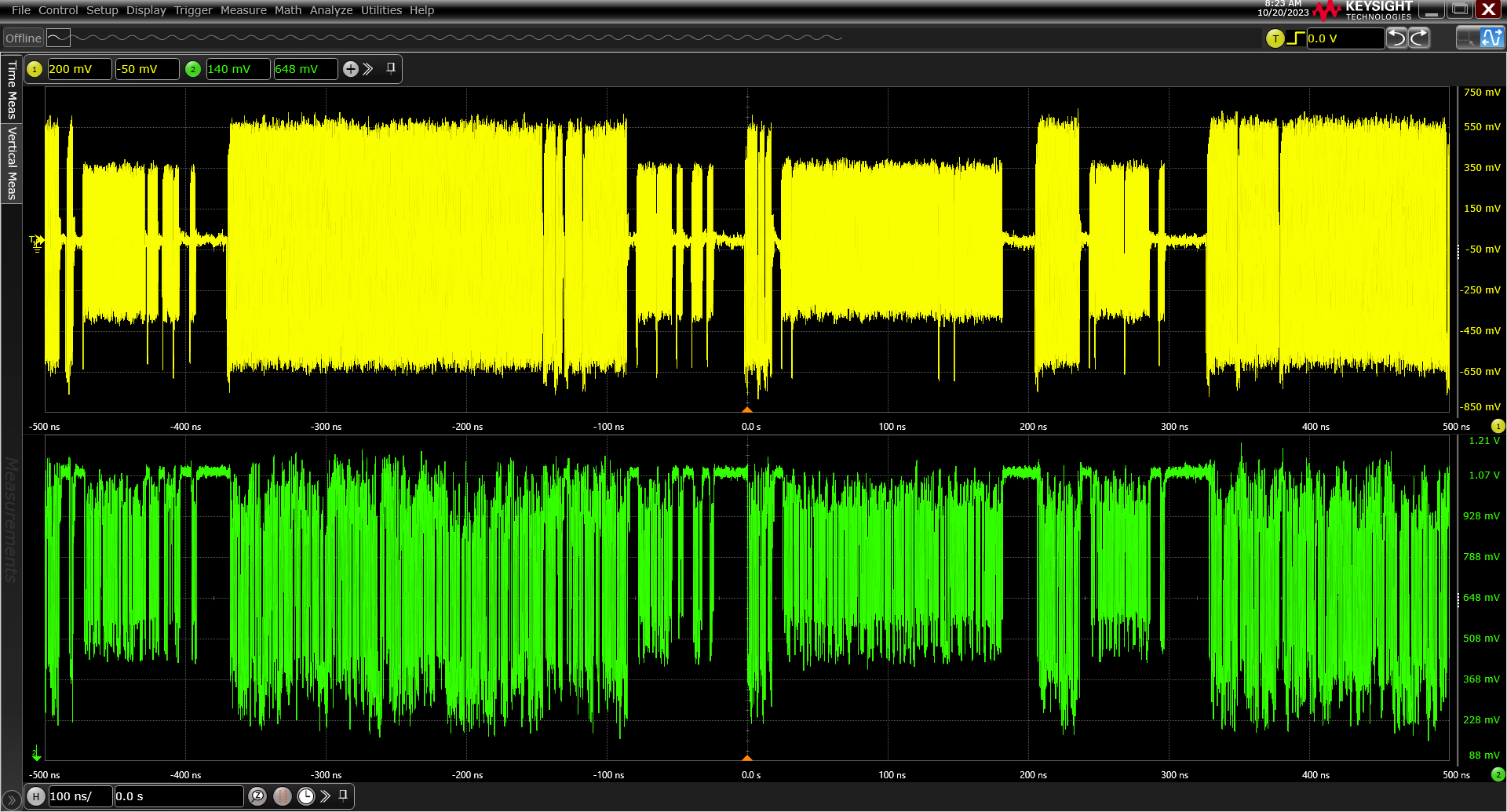 Figure 7. Higher amplitude DDR5 read bursts vs. write bursts (20% higher read than write amplitude).
Command/Address Decode
Since the DRAM receives command and address information for read and write transactions it seems natural to think that test equipment could also decode commands to better identify bursts. This is the ideal scenario and works for some configurations. The most obvious and effective setup is to use a mixed signal oscilloscope that includes four analog input channels and 16 or more digital input channels. This setup has been used in several applications successfully with the main drawbacks being setup complexity and added expense for the additional digital channels.
An alternative to the full command bus decode option is to partially decode the CA bus and focus only on the CA bits that determine the burst type for a given command. For DDR5, this is CA4.
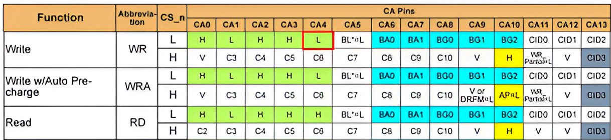 Figure 8. Partial DDR5 command truth table showing CA4 signal always low for a write command vs. high for a read.
Example Workflow
Thresholds and Reference Timings
The next section will provide an overview of an example workflow to prepare for measuring reads and writes. This section covers properly setting up thresholds and configuring the burst timing parameters.
Thresholds or reference levels are used to determine valid transitions at the start and end of a burst as well as between the DQ and DQS signals. Figure 9 below shows a Read burst followed by an electrical idle state then a Write burst.
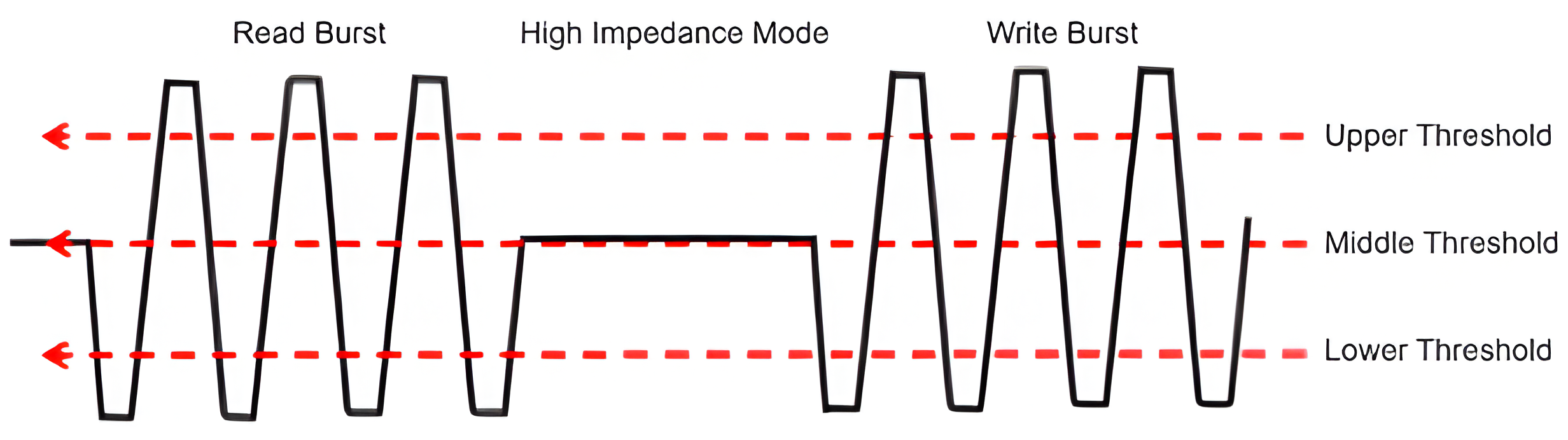 Figure 9. Thresholds used to determine valid transitions.
Not all thresholds are used for the same purpose. The upper and lower thresholds, for example, might be used to detect the presence of any type of burst. In the case of the high impedance mode when no data is present in Figure 9 the signal does not cross the upper threshold. However, when performing timing measurements within a burst the middle threshold might be used.
Measurement Setup
In addition to the thresholds it’s also important to configure the proper timings such as pre- and post-amble lengths, clock frequency, and CA4 read or write command latency (if used). Let’s go through an example to show how this works.
Step 1: Identify timings and reference levels by using on screen markers or cursors to measure delays and pre- and post-amble transition voltages. Notice in Figure 10 CA4’s (red) latency at the start of the valid Write burst (green).

Figure 10. Clock, strobe, data, and CA4 signals.
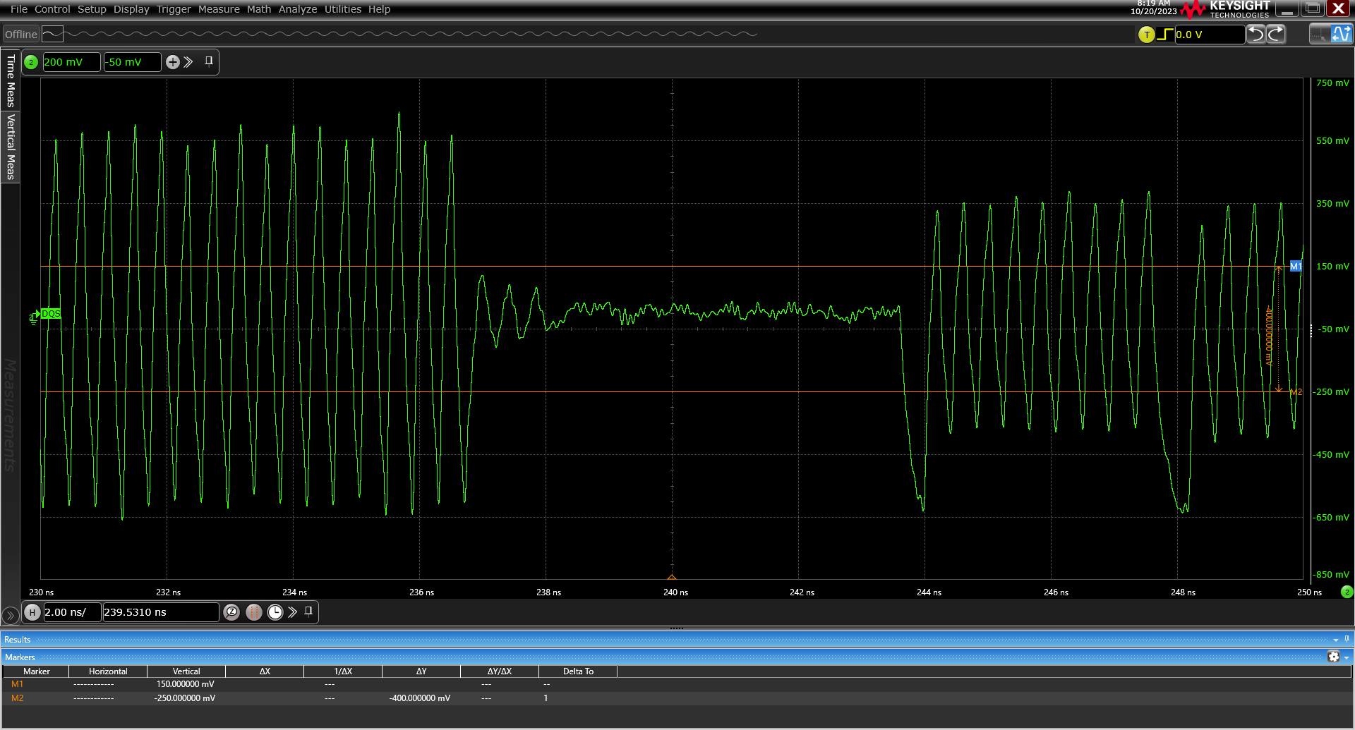 Figure 11. DQS signal threshold level measurement.
Step 2: Enter thresholds, timings, speed and signals used in your test application.
 Figure 12. DDR5 compliance app setup.
Step 3: Select and run tests.
 Figure 13. Test selection.
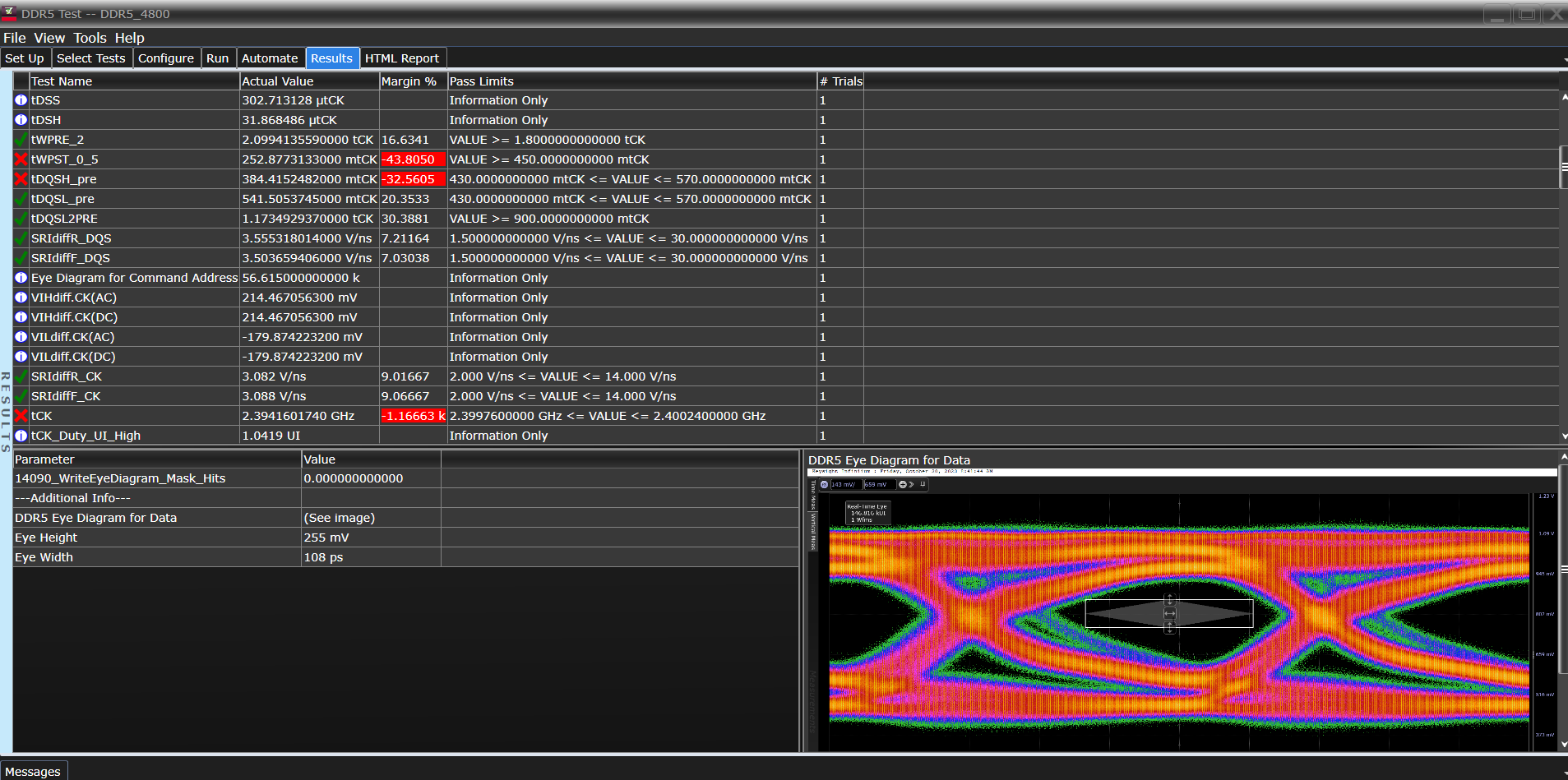
Figure 14. Results view.
A quick assessment of the test results reveals that some of the results are outside the specification tolerance. For further investigation it’s recommended to verify test settings (including thresholds and timings), confirm results per specification references and possibly explore additional system trainings or adjustments as needed to improve overall margin.
Summary
One of the most important steps in memory test is ensuring that the right data is being analyzed. There are challenges and techniques involved in separating read and write data bursts in DDR5 memory systems. DDR5 aims to enhance memory performance, and the higher data rates the standard supports present the need for efficient burst separation. Common methods for achieving this include phase alignment, amplitude differences, and command/address decoding. Following a standard workflow for setting up thresholds and timings to distinguish bursts in DDR5 memory interfaces can make design validation much more efficient. This will ultimately ensure compliance with specifications and improve system margin by identifying and resolving any issues, especially those that are related to either read or write transactions.
REFERENCES