
This paper is an Outstanding Paper Award Winner from EDI CON USA 2017.
Power distribution networks (PDNs) delivering power to ICs in a system need to be thoroughly designed and analyzed in order to make sure any voltage fluctuation on the rail is within the tolerance of every IC connected to that rail. As ICs on the rail draw power, they generate a voltage fluctuation on the rail. The PDN must have the capacity to supply enough charge such that the resulting voltage drop is less than the maximum voltage drop each IC on the rail can tolerate. If voltage fluctuations appear outside IC tolerance limits, a slew of problems can surface such as IC damage, failure, or reduced lifespan.
Currently, the leading systematic PDN design approach is the target impedance methodology [1]. The target impedance approach is a good approximation for the worst-case voltage fluctuation on a rail given the maximum current load anticipated on that rail. However, unless the impedance profile is perfectly flat and linear, the target impedance methodology is only an approximation because it does not consider phase and the possible coupling of different resonances. These can contribute to a higher voltage fluctuation than the target impedance design methodology predicts. Building a flat impedance profile within a necessary bandwidth is possible but complicated, and often not worth the added cost. An example of an achieved flat impedance profile from [2] is shown below in Figure 1. The effects of the unmitigated resonances on voltage fluctuation magnitudes must be captured in the validation process in order to guarantee the rail voltage remains within the tolerable range. Power integrity engineers are looking for a time domain PDN validation strategy to compliment the frequency domain validation approach for this more thorough PDN analysis [3].

Figure 1: Measured data collected from a CPU core rail of a server computer board illustrating an achieved flat impedance profile.
This paper examines a transient load test (TLT) tool developed for time domain PDN validation. Using clever circuit layout strategies and the new Gallium Nitride (GaN) FETs beginning to be developed by companies [4], we have been able to develop a compact, high slew-rate circuit that loads a device under test (DUT) with an arbitrary current waveform defined by a connected signal generator. The TLT allows for a thorough characterization and analysis of the PDN in the time domain. This transient load analysis does not have the same linearity and flat profile assumptions that the target impedance methodology assumes and so allows the design engineer to capture information about the behavior of the PDN that frequency domain analysis cannot easily supply. This time domain approach allows for a comprehensive analysis of the behavior of the PDN in system as if the CPU were in place.
Transient Load Tester Circuit Architecture
The TLT is designed to be connected directly to a DUT and generate a load current that follows an input signal from a signal generator. The TLT’s circuit topology is shown below in Figure 2. The TLT consists of a GaN FET driven to load the DUT. The driving circuit consists of a high-speed op amp driving a class A buffer circuit, which in turn drives a GaN FET. A current sense resistor is connected to the source of the GaN FET and the voltage over the sense resistor is fed back to the inverting terminal of the op amp to close the loop around the circuit. The non-inverting terminal of the op amp is driven by a signal generator, which the load current waveform on the DUT then follows.
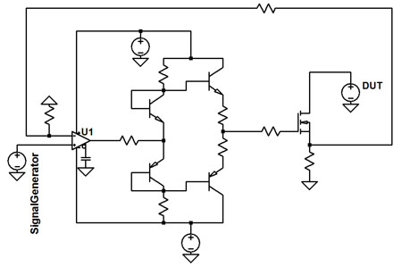
Figure 2: TLT circuit architecture with approximate component values.
The goal of the TLT design is to be able to load a DUT with as large a current as necessary and as fast as necessary. The high-speed op amp was chosen for this reason. A class A buffer was built between the op amp and the gate of the GaN FET so that the op amp would not have to drive the capacitive load of the GaN FET gate directly as this could lead to stability issues. Finally, the GaN FET was chosen because its high performance electrical characteristics make it advantageous to use over the traditional silicon power FETs. The GaN FET allows for the high-speed circuit operation we are looking for.
A current offset bias circuit was included and connected to the inverting input node of the op amp. It is important that the FET be slightly on during the TLT operation. The reason for this is to minimize the voltage slew the TLT needs to exert in order to turn on the FET and load the DUT. This helps to optimize the speed at which the TLT operates. The low threshold voltage of the GaN FET aids in achieving a faster turn on time by helping to further minimize voltage slew as well. In this TLT design, the offset bias circuit was configured such that when the TLT is “off,” it loads the DUT with 1A current.
The GaN FET
The GaN FETs available on the market come in two flavors: depletion mode and enhancement mode. Depletion mode GaN FETs have been available on the market for a while now but have inherent dangers in operation since their “off” state with no gate voltage applied, they are “on” or effectively a short. If a depletion mode GaN FET were used in the TLT design and there was a malfunction with the supply voltages, the control loop, or the drive circuit, the depletion mode FET could easily short the DUT and damage the DUT as well as the TLT. High speed, enhancement mode GaN transistors with electrical characteristics that largely outperform the traditional silicon power MOSFETs are now available on the market. Enhancement mode FETs are effectively an “open” when there is no gate voltage supplied and so were chosen for the TLT for safety.
An enhancement mode GaN FET was considered and ultimately decided on for the TLT project [5]. The maximum ratings for this FET are shown below in Figure 3.

Figure 3: Maximum ratings for enhancement mode GaN FET considered for TLT [5].
Figure 4 shows the cross-section of the GaN FET structure from [6]. The GaN FET is built starting with a silicon wafer as the substrate. A thin layer of Aluminum Nitride (AlN) is grown on the silicon wafer to isolate the device. A layer of GaN is grown on the AlN layer, followed by a thin layer of Aluminum Gallium Nitride (AlGaN). The AlGaN layer strains the piezoelectric GaN layer and generates a two-dimensional electron gas (2DEG) at the interface. This 2DEG is a fantastic trait of the GaN FET because it has super low resistivity. Finally, a depletion region under the gate is formed and metal layers are added to the source, drain, and gate terminals.
As shown in Figure 5 from [7], the lateral structure of the FET means CGD is generated by a small corner of the gate such that CGD is exceptionally small in value. CGS is large compared with CGD, but still less than the corresponding CGD seen with silicon MOSFETs. Since gate charge (Qg) is a function of CGD and CGS, the Qg of the GaN FET is low compared to that of silicon FETs. A silicon power FET rated for a VDS of 40V and a continuous drain current of 49A was also considered for the TLT because of its fast switching characteristics [9]. For switching comparison, the GaN FET’s input capacitance at VDS = 20V and VGS = 0V is nominally 980 pF and at VDS = 20V and ID =33A its total gate charge is nominally 8.7 nC [5] whereas the silicon FET has a nominal input capacitance of 1400 pF at VDS = 20V and VGS = 0V and total gate charge of 18 nC [9] at VDS = 20V and ID = 30A. The GaN FET’s low Qg allows for short delay times and fast switching speeds with high precision. Integrating this GaN FET into the TLT design gives the TLT the exceptional advantage of loading of the DUT with a fast slew rate.
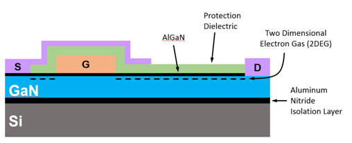
Figure 4: eGaN FET Structure from [6].
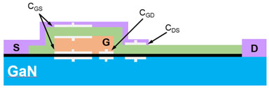
Figure 5: Effective capacitances of eGaN FET Structure from [7].
The TLT design also aimed for the FET to have as small of a threshold voltage as possible. As shown in Figure 1, much of the voltage drop in the TLT’s current loading path comes from the current sense resistor and other parasitic resistances in the load current path. The DUT voltages expected for this TLT project’s application are expected to be around 1V. The voltage drop over the sense resistor compresses the maximum VDS and VGS achievable and so limits the maximum current loading capabilities of the TLT. The GaN FET is rated for threshold voltages between 0.8V and 2.5V with a nominal threshold voltage of 1.4V. For comparison, the silicon FET is rated for a threshold voltage between 1.2V and 2.0V. The RDS(ON) of the GaN FET is also slightly less than its silicon MOSFET counterpart. The GaN FET considered for instance at Tj = 25 ○C, VGS = 5V, and ID = 33A has a typical RDS(ON) of about 4 mΩ [4] whereas the silicon FET considered has a typical RDS(ON) of about 14 mΩ. This further increases the voltage available to VDS for the GaN FET considered, improving the maximum current loading capabilities of the TLT using this FET.

Figure 6: Land grid array package layout of GaN FET from [8].
Finally, the considered GaN FET’s package is laid out in a land grid array as show in Figure 6 from [8]. This layout reduces the common-mode high-frequency loop inductance which leads to cleaner high speed TLT operation as well.
The Transient Load Tester Implementation and Test Results
The fully constructed TLT is shown below in Figure 7. The testing carried out on the TLT was collected while the TLT was connected to a capacitor bank which was in turn connected to an electronic bench supply. The TLT was driven by an arbitrary waveform generator connected via coaxial cable. Figures 8 and 9 show the TLT’s following behavior during operation by comparing the voltages on the inverting and non-inverting terminals of the op amp. The voltage waveform on the inverting terminal corresponds to the current loading the DUT, multiplied by the sense resistance and divided by the gain of the op amp configuration. In this case, the sense resistance is 10 mΩ and the gain of the circuit is 11. The measurements shown in Figures 8 and 9 were collected while the DUT voltage was 1V. The rise and fall times of the input voltage waveform were 100 ns, each. The voltage at the non-inverting terminal of the op amp shows the input waveform that the load current was intended to follow.

Figure 7: Fully constructed Transient Load Tester connected to capacitor bank.
For a DUT voltage of 1V, the TLT was able to load the DUT with up to 30A before the load current waveform started to degenerate as shown in Figure 8. In Figure 9, the rising edges of the input voltage waveforms and the load current waveforms are zoomed in on. Although there is a delay between the input voltage waveform and the load current waveform, the load current waveform rose at 100 ns following the input voltage waveform.
The limitation on the amount of current a single TLT circuit can load is largely dependent on the supplied DUT voltage and parasitic resistance in the load current path. Figure 10 shows (a) a clean 20A load step and a degenerate 40A load step for a DUT supplying 1V, as well as the corresponding VDS and VGS in (b) for each case. In the 20A case, VGS and VDS are clean. In the 40A case VDS drops as low as 29 mV as much of the voltage supplied is consumed by the sense resistance and stray resistances in the DUT-TLT current path.

Figure 8: Comparison of voltages at inverting and non-inverting input of op amp during TLT operation with DUT output voltage of 1V.

Figure 9: Comparison of voltages at inverting and non-inverting input of op amp during TLT operation captured from 0 to 0.5 µs with DUT output voltage of 1V.
The closed-loop circuit hits the inherent limitation in which the feedback circuit increases VGS in order to increase the load current, but the voltage drop from path resistances increases as the load current increases. This compresses VDS and results in a lowering of the load current. This process of the TLT circuit fighting and ultimately converging on its limited maximum current is seen in the 40A and 50A step cases in Figure 8, and is responsible for the poor stability and degenerate wave shape of the 40A case in Figure 10. A lab bench supply was used as the DUT for these measurements. The lab bench supply inherently requires more series DC resistance in how it is connected to the TLT than a normal DC-DC converter would require. In cases of cleaner connections to the TLT, a higher maximum load current can be achieved than what is shown in Figures 8 and 10.
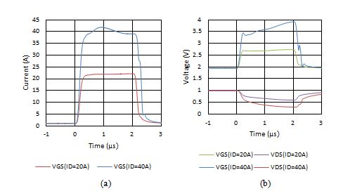
Figure 10: For a DUT supplying 1V: (a) 20A load and 40A load current generated by TLT; (b) VGS and VDS corresponding to the 20A and 40A current load.
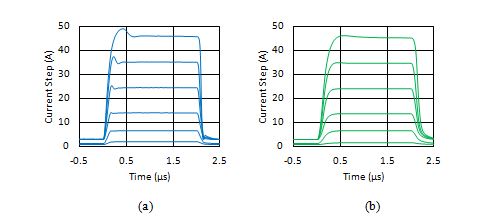
Figure 11: Input voltage waveform and corresponding current load waveform scaled to voltage seen at inverting terminal of op amp for: (a) TLT board #1, (b) TLT board #2.
The limitation on the maximum load current a single TLT circuit can achieve has a simple fix. More current can be loaded by operating multiple TLT circuits in parallel. For example, four TLT circuits can be coordinated to load a DUT at 25A each, which is equal to loading the DUT with a 100A current pulse having the same clean shape seen when a single TLT circuit is loading only 25A. Figure 11 shows the current loading behaviors of two separate TLT circuits when independently loading a DUT. Figure 12 shows the current loading behaviors of the same two separate TLT circuits as they load the same DUT at the same time. The current loading behavior of each TLT circuit is not influenced by the fact that they are loading the same DUT at the same time. By distributing the load over multiple TLT circuits operating in parallel, the maximum load current becomes virtually unlimited by the TLT and only constrained by the limitations of the DUT.

Figure 12: Input voltage waveform and corresponding current load waveform scaled to voltage seen at inverting terminal of op amp for TLT board’s #1 (in blue) and #2 (in green) connected to same DUT and operating in parallel.
Further TLT Considerations for Implementation
Ultimately, the final transient load circuit, composed of the multiple TLT circuits in parallel, is best to implement in PCB form so as to minimize stray capacitances and inductances and achieve the fastest and highest quality performance. There are a few other variables that need to be considered, however, when designing a compact PCB solution.
In the implementation of the several TLT circuits in parallel, the FETs and current loading loops all need to be close to one another in order to minimize path resistance in the load current loop. This will also force the TLT circuit to get exceptionally hot, especially in the region in which the FETs are located. A single TLT circuit was connected in a temperature test chamber to a DUT supplying 1V, and the current loading behavior corresponding to a load pulse with a 100 ns rise time was measured at different temperatures as shown in Figure 13.
Fortunately, the effect of temperature on the current loading wave shape is seen to be minimal as there is little variance between waveforms. The implementation of several TLT circuits in parallel in a single PCB also limits the minimum distance between the gate driving circuitry and the gate of the FETs. Since all the FETs should be located close together, it is likely infeasible to design gate-driving circuitry into the PCB that will connect to corresponding FETs within a few inches in the cases of all the FETs. Coaxial cables of different lengths were connected in between the gate drive circuitry and the gate of the GaN FET.
The current loading behaviors for different length coaxes were measured for a DUT supplying 1V and the results are shown in Figure 14. The fear is that too long of a distance between the gate drive circuitry and the gate of the FET could induce enough of a phase shift to cause stability degradation. However, as seen for even the case of 10 inches, there is virtually no difference in performance. This makes sense as a 10 inch coax causes approximately 1.2 ns of delay which is almost unobservable here as the rise and fall times are at least 100 ns and the duration of the pulse is even longer. In a PCB trace, the delay will be slightly larger since the speed of a signal in a PCB trace is slower than in a coaxial cable. However, given the size of the components, a PCB layout should be achievable that gives little enough delay in the gate drive communication to avoid stability issues.
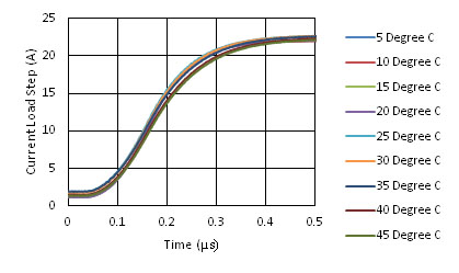
Figure 13: TLT current load step behavior for coax cables of different lengths inserted between the gate drive circuitry and the gate of the FET.

Figure 14: TLT 20A load step behavior with 100 ns rise time for coax cables of different lengths inserted between the gate drive circuitry and the gate of the FET.
TLT Usage for DC-DC Converter and its PDNs Time Domain Performance Testing
The implementation of the TLT in PCB form allows for the testing of a DC-DC converter and its corresponding PDN. The fundamental worries with PDN design are that the PDN cannot supply the necessary current to the devices on the rail and that the voltage drop or fluctuation on a rail due to a step in current will not remain within the tolerances acceptable to the devices on the rail.
If the appropriate amount of current cannot be sourced, the connected devices cannot operate correctly. If voltage drops or fluctuations are too big, then chips can become damaged and length of life cannot be guaranteed. The TLT allows the designer to observe the dangers posed by these issues in his design, directly. The engineer can set the TLT to load the PDN with a pulse train of a magnitude equal to the maximum current the rail must support. The engineer can then vary the frequency and duty cycle of the pulse train to observe the worst case voltage ripple due to the current load steps as the fluctuation is exacerbated by resonances and even the constructive interaction of different resonances.
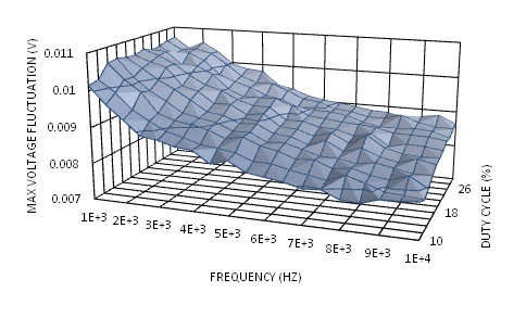
Figure 15: Peak-to-peak voltage fluctuation on output of DC-DC converter due to 15A load pulses as a function of frequency and duty cycle.
Figure 15 shows an example of a DC-DC converter’s output voltage as the converter was loaded by a 20A pulse train while the frequency and duty cycle were varied. The TLT emulates the worst-case operating conditions the PDN must support within a live system, giving the design engineer a thorough glimpse of the designed PDN’s real performance. In the future, the step response collected from the TLT can be used to reconstruct the impedance profile of the PDN and the worst case voltage fluctuation achievable according to the reverse pulse technique [10].
The design of a transient load test circuit that can load PDNs with currents at the speed and magnitude anticipated in system is now achievable thanks to the exceptional electrical performance of power GaN FETs on the market. The implementation of the GaN FETs with clever circuit design has allowed for the achievement of a high-bandwidth closed-loop circuit that can load a DUT with a current pulse of up to 100 ns rise and fall time and virtually unlimited maximum current. The TLT tool allows for the simulation of worst case loading conditions on a PDN in system within a lab setting. This ultimately allows higher quality PDN design than can be currently achieved by simply designing to the target impedance since the worst case ripple on a rail in system can be investigated in the lab.
Author(s) Biography
Ethan Koether is a Hardware Engineer at Oracle Corporation. He is currently focusing on system power-distribution network design, measurement, and analysis. He received his master's degree in Electrical Engineering and Computer Science from the Massachusetts Institute of Technology.
Istvan Novak is a Senior Principle Engineer at Oracle. Besides signal integrity design of high-speed serial and parallel buses, he is engaged in the design and characterization of power-distribution networks and packages for mid-range servers. He creates simulation models, and develops measurement techniques for power distribution. Istvan has twenty plus years of experience with high-speed digital, RF, and analog circuit and system design. He is a Fellow of IEEE for his contributions to signal-integrity and RF measurement and simulation methodologies.
Acknowledgement
The authors wish to thank for their help Kavitha Narayandass, Alex Miranda, Guy Phillips, Dan Sullivan, Dave Michaud, Bill Tata, Khan Nguyen, Dan Rich, Randy Luckenbihl, Jerome Gentillet, Sandra Brescia, Raja Burney, Gustavo Blando, Laura Kocubinski, all of Oracle Corporation.
References
[1] Steve Sandler, “Target Impedance Limitations and Rogue Wave Assessments on PDN Performance,” paper 11-FR2 at DesignCon 2015, January 27 – 30, 2015, Santa Clara, CA.
[2] “Controlled-ESR Bypass Capacitors Have Arrived” in TecForum TF-MP3 at DesignCon 2007, January 29 – February 1, 2007, Santa Clara, CA
[3] S. Chickamenahalli, et al., Microprocessor Platform Impedance Characterization using VTT Tools, Applied Power Electronics Conference and Exposition, 2005. APEC 2005. Twentieth Annual IEEE. Vol. 3. IEEE, 2005.
[5] EPC2015C – Enhancement Mode Power Transistor Datasheet. http://epc-co.com/epc/Portals/0/epc/documents/datasheets/EPC2015C_datasheet.pdf
[6] A. Lidow and J. Strydom, “Gallium Nitride (GaN) Technology Overview”, 2012. http://epc-co.com/epc/Portals/0/epc/documents/papers/Gallium%20Nitride%20GaN%20Technology%20Overview.pdf
[7] A. Lidow and M. Rooij, “eGaN® FET Electrical Characteristics”, 2012. http://epc-co.com/epc/Portals/0/epc/documents/papers/eGaN%20FET%20Electrical%20Characteristics.pdf
[8] J. Strydom et. al, “Using Enhancement Mode GaN-on-Silicon Power FETs (eGaN® FETs) 2014. http://epc-co.com/epc/Portals/0/epc/documents/product-training/AN003%20Using%20Enhancement%20Mode%20GaN-on-Silicon.pdf
[9] OptiMOSTM3 Power-Transistor Datasheet. https://www.infineon.com/dgdl/Infineon-BSC093N04LSG-DS-v02_01-en.pdf?fileId=db3a30431689f4420116c44a1fa80822
[10] Jae Young Choi, et al., “Electrical and Thermal Consequences of Non-Flat Impedance Profiles” DesignCon 2016, January 19 – 21, 2016, Santa Clara, CA.