
The PDN impedance in the milliOhm range can be measured with Vector Network Analyzers (VNAs) using two-port shunt-through connection. Measuring impedance in large pin-fields, where one or both sides of the supply rail use only blind vias, requires same-side probing. When the two ports are in close proximity the crosstalk/coupling between probe tip loops alter the results. The coupling between the probe tip loops can be de-embedded or calibrated out based on its equivalent circuit, but it still leaves the effect of coupling between the via-trace structures from the landing points to the planes down in the stackup (see Figure 3).

In this article, we will investigate via and trace coupling effects using measurements, hybrid, and full-wave solvers by de-embedding/calibration utilizing multiple test-boards.
Two-Port Shunt-Through Measurements
Measuring impedance using a single port is only accurate for impedances above 1 Ω due to load to port mismatch and parasitic of launch masking lower impedances. To get around this issue, we use a two-port shunt-thru measurement. Figure 1 shows the two-port technique where port 1 drives the current through the DUT, and port 2 measures the voltage.
 Figure 1. Schematic of two-port shunt through measurement setup.
Using two ports to obtain S21 will give us a much more accurate measurement of the low impedance of the DUT power rails, also because transmission measurements tend to have higher dynamic range than reflection measurements.
We can also extract from the S Parameters the Z matrix, then converting in a more convenient description of the DUT by T equivalent circuit.1
The T-circuit transformation eliminate the probe series parasitic to derive the shunt element ZC , which represents the DUT. However, the actual ZC term is impacted by mutual coupling within the PCB launch area. Simply having two orthogonal loops does not guarantee zero magnetic coupling. To minimize both electric and magnetic coupling, full symmetry is required (see Figure 2).
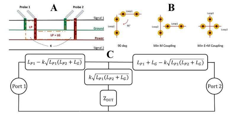 Figure 2: Two-port shunt measurement and parasitics, after Z to T Transform. (A) Side view of measurement setup showing inductive loops. (B) Top view of via structures with inductive loops at 90⁰, perpendicular to minimize magnetic coupling, and crossing to minimize both electric and magnetic coupling. (C) Relationship between coupling and loop parameters shown on the top left to the T-network. InFigure 2,LPis assumed to be the inductance of the power/ground via pairs extending the physical probes, and both launches are assumed to be identical with a coupling of kbetween the via current loops. LGrepresents the plane inductance between the launch vias. There is a term folding intoZCstemming from the via coupling where the system is probed. We have to remove this term. The mathematical relation connectingZDUTwithS21and the parasitics from the probe launch is as follows.6
We need to find the different inductive terms and their coupling coefficient.
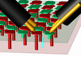 Figure 3. 3D simulation setup of area of probe landing. Two ports at the coax RP probe and a port in the center representing the DUT. Power plane gap has been artificially expanded for illustration purposes.The method we implement in this paper is to see the launch as a series extension of the DUT. We will de-embed from the probe pads to a port exactly between the pads (the blue vertical rectangle in Figure 3), using an extracted model of the launch structure. The method will not change how we probe or calibrate in the lab, but would add a post-processing step. The methodology creates several challenges related to ensuring that the extracted PCB launch model properly represents what is being measured in the lab, considering that the model is dependent on probe angle, spacing, offset, and probe orientation as well as the measurement environment.
 Devices Under Test
Three different boards have been used in our analysis.
Solid Copper Sheet
 Figure 4. Photo of the copper sheet.
To minimize the number of variables, the tests started with the probes landed on a rectangular piece of solid copper sheet. Between two contact point, the resistance of the sheet can be calculated from analytic expressions.
Test Board With 8x8 Via Arrays
 Figure 5. Photo of probes landed on an array on the right.
The test board 8x8 via arrays used has 20 layers and five power-ground cavities. One via through-hole via array (J0401) was measured. The vias connect the second and third layers (see Figure 5). The inductance of the structure was measured by looking at the impedance at the center of J0401 via array.
Note that the via array has a checker-board pattern alternating power and ground connections, which requires the probes to be in opposite orientation (called flipped in this document) facing each other with no offset.
Customer Demonstration Board With 1mm BGA Via Field
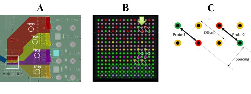 Figure 6, Customer demonstration board power plane assignment (A), close-up of the measured BGA pinfield (B), and the probe landing pattern showing the offset and spacing between the probes (C).
Simulating Low Impedance PDN Configurations
Extracting models of low impedance configurations naturally requires consideration of all parameters that go into the extraction tool as well as the actual extraction method. Stack-up parameters such as thicknesses should be adjusted along with process parameters such as plating thickness and material properties properly calibrated (specifically conductor electrical conductivity and dielectric constant). Today, a majority of PDN simulations are done in hybrid EM simulation environments. The hybrid methods decompose the board behavior into plane modes, transmission line modes, and localized discontinuity models like vias and padstacks.
Decomposition makes the extraction very fast and is capable of handling even the most complex board layouts being designed today. However, when it comes to studying very detailed and localized behavior, typically around field transition areas, the user must be careful with solvers that use the hybrid method and should correlate results in a full-wave 3D electromagnetic extraction. The present work is primarily concerned with the frequency range on a PCB where sub-mΩ resistance may be achieved and thus where the local distribution of currents is a key in understanding the realized resistance. Users also must be careful applying typical full wave 3D solvers as these normally apply skin impedance boundary conditions and other higher frequency oriented settings. The transition from bulk current conduction mode to the skin depth dominated conduction mode is of key importance to the accuracy of the simulation, and a volume mesh for the conductors may be required to properly resolve the redistribution of currents as we go from the very low frequency behavior towards the skin depth dominated region.
When simulating impedances in the µΩ range, the results can be very sensitive to a variety of physical parameters. Performing sensitivity analysis is important to understand which parameters will have the biggest impact on the results.
We realize there are three key parameters that can be changed that will have a profound effect on the DC resistance of the simulated structure:
- The sheet thickness (TH)
- How deep the probe goes into the metal (probe offset, OFF)
- Surface roughness of copper (SR).
To determine the best fitting of these variables to get a good match to our measurement results at DC, we ran a Design-of-Experiment with the identified variables.
We saw that the metal sheet thickness has the highest sensitivity with a maximum sensitivity at the mid-point of the range of thicknesses. The probe offset and surface roughness have approximately the same sensitivity, and both show little contribution to the low frequency impedance.
Measurement Considerations
A VNA E5061B model with low-frequency extension was used. VNAs can measure low impedance in Two-port Shunt-through configuration , but we need to be careful to suppress the low-frequency error created by the loop formed by the two cable shields. To meet these requirements, for measurements in the 100 Hz to 10 MHz range two half-meter long PDN cables were used to connect the VNA to the probes. This length was a comfortable minimum to reach from the VNA to the probes and these cables have low braid resistance and are also very flexible.
To further reduce the low-frequency cable-braid error, a common-mode choke was used, but to achieve the highest possible dynamic range, a home-made toroid common-mode choke was created for our setup using a nano-crystalline alloy core.
In the GHz frequency range, the DC resistance of the cable braid matters much less and therefore in the setup covering the 2 MHz to 3 GHz range, we used high-frequency cables. Probing printed circuit boards for PDN measurements requires robustness and not necessarily a very high bandwidth. The single-ended probes used have a symmetric construction, allowing us to use the same piece for either G-S or S-G probe configuration. To perform calibration, we had two options: to calibrate to the end of the coax cables with an electronic calibration kit, or to calibrate to the tips of the probes with a wafer-probe calibration substrate.
 Figure 7. Planarizing and aligning the probe tip.
The probe-tip coupling values also depend on the probe spacing, parallelism and the landing angle of the two probes. The equipment available limited our choice of the landing angle to a single value, 45°, so far.
Measurement to Simulation Correlation
To determine how well we are able to extract the DUT impedance from our PROBE-DUT-PROBE measurement and simulation results, we look first at our correlation results for the shorted case on a piece of copper.
 Figure 8. Measurement-to-simulation correlation for probes on copper sheet. Probe impedances for six configurations.
For these simulations, there are two probes on the top, with 1 mm separation between signal and ground per probe. This shorting sheet will allow us to understand and correlate the circuit R and L. We are using a full-wave 3D solver and a quasi-static solver.
Figure 8 shows that the inductive correlation in the measured and simulated probe impedance is very similar across six permutations. The fact that all six results match suggests that the T-network extraction is performed correctly.
Test Board With Via Array
The test board was simulated using two different approaches: a Hybrid EM tool and a 3D FEM simulator. Figure 9 shows the frequency-dependent resistance and inductance derived from the simulations. The graphs show both R and L derived from the T-transformation DUT representation (ZC) as well as the values for the internal port.
 Figure 9. J0401 center location resistance (A) and inductance (B) plot from Hybrid EM and 3DFEM simulations. Both ZC transformation and buried ports are shown. Resistance (C) and inductance (D) correlation for ZC data.
 Starting with the correlation data in the lower frame of Figure 9, we see a reasonable agreement of resistance and inductance compared to the measurements (the buried ports should not be considered in such comparisons). Also, we note that the results from the different EM simulators agree quite well with the most variation in the inductive region and beyond.
Customer Demonstration Board
The board was measured in the BGA pin-field at the location that was identified in Figure 6. The good agreement with wafer-probe calibration without isolation calibration step demonstrates that interconnect delay added in any of the two legs of the two-port shunt-through measurement outside the calibration loop does not noticeably change the result as long as the extra attenuation is low and the added pieces are electrically short.
 Figure 10. Measured and simulated rail impedance of customer demonstration board. Impedance magnitude (A) and extracted inductance (B).
Conclusion
From a simulation standpoint, we have covered several important topics that users must consider in detail to get accurate low frequency simulation results. We investigated solver and mesh topics, variable sensitivity, and what to expect regarding the low frequency results. We showed that good correlation can be achieved between simulation and measurement for several cases.
Finally, we have established a methodology for using simulation results to post-process measurements in order to remove coupling inherent in a launch structure from the two-port probe measurement methodology. We achieved a substantial improvement in power-rail inductance correlation for a BGA pinfield by analyzing the contributors to the errors.
The paper referenced here received the Best Paper Award at DesignCon 2023. To read the entire DesignCon 2023 paper, download the PDF.