
Printed-circuit-board (PCB) connectors come in all shapes and sizes and are used across multiple applications. They can be classified as either board-to-board connectors, which enable the backplane and daughter card architecture, or board-to-cable connectors, which connect wiring to a PCB. PCB connectors are also characterized in terms of gender. A male connector, or plug, comes with a specified number of pins, while a female connector, or receptacle, contains sockets that mate with the pins of the male connector.
PCB connector suppliers are often tasked with providing connectors that meet today’s high-speed and high-density requirements. In many cases, these connectors also need to maintain signal integrity under harsh conditions. One company that is focused on meeting all these demands is IEH Corporation, which provides a wide range of PCB connector solutions. The company’s hyperboloid interconnect products are intended for aerospace, defense, commercial, and medical use.
Incorporating a connector into a design requires a good simulation model for the connector if the designer intends to simulate real-life performance. Such models make it possible to simulate how the connector will interface and perform in its surrounding environment1. In particular, for high-bandwidth applications, it is critical to have accurate models to simulate the connector together with the PCB. One specific area of concern is crosstalk, which may not be predicted correctly unless the PCB and connector are simulated together. Oftentimes, these simulations are not performed due to the considerable simulation requirements that result from the large pin counts typically associated with these connectors. The proprietary nature and complexity of the connector designs represent additional challenges.
Modelithics 3D Connector Models
IEH has partnered with Modelithics® to offer 3D geometry models for various IEH hyperboloid connector products as shown in Figure 1. The models are intended for designers looking to perform 3D simulations of PCB-based designs.

S-parameters were simulated in both single-ended and differential mode for all Modelithics 3D models for IEH connectors. The models are validated to either 20 or 40 GHz. For each model, time-domain data is generated through fast fourier transform of S-parameter data.
The models also include a new feature called “Dynamic Region Selection” that lets users isolate specific rows and columns to include in a simulation2. With this feature, objects not included in the selection are still visible but are assigned the “non-model” property. These “non-model” objects are excluded from the simulation, thus reducing the overall simulation time and resource requirements.
Single-Ended and Differential S-Parameter Simulations
Various simulations can now be shown to demonstrate the functionality of the connector models. Note that the simulation results presented here correspond with the expected connector performance documented by IEH. One can contact IEH for more information regarding connector performance.
As mentioned, the S-parameters of all the 3D models were simulated in both single-ended and differential modes. To demonstrate, Figure 2 shows a configuration used in Ansys HFSS to perform a single-ended S-parameter simulation. This simulation project includes the HMK200MDA3A97E5C male connector attached to the HMK200FDA3A98E5C2 female connector. PCBs are attached to the other side of both connectors. The substrate used here for the PCBs is 15-mil Rogers RO4350B (microstrip configuration) on top of a single layer of the same substrate set to an arbitrary thickness of 134 mils. Figure 3 shows the simulated insertion loss and return loss up to 5 GHz. The results show that the insertion loss remains within 2 dB all the way to 5 GHz. Figure 4 shows the PCB up close to reveal the location of the reference plane used for the simulation.
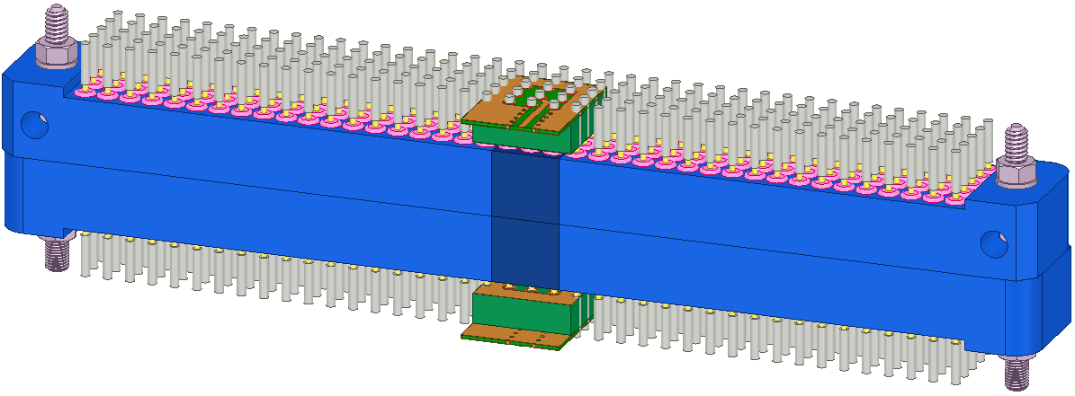 Figure 2. HFSS configuration used to perform a single-ended S-parameter simulation. The HMK200MDA3A97E5C male connector is attached to the HMK200FDA3A98E5C2 female connector.

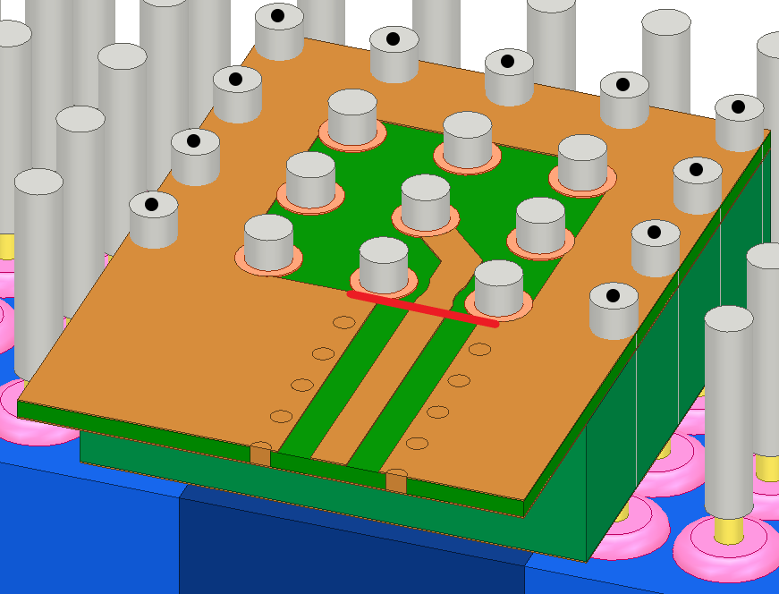 Figure 4. For the simulation, the ports were de-embedded to the location shown by the red line. Note that the pins with the black dots (and the pins not attached to the PCB) are assigned the “non-model” property using the “Dynamic Region Selection” feature. Hence, although these pins appear visually, they are excluded from the simulation.
Figure 5 shows the simulated time-domain reflectometry (TDR) of the single-ended configuration. For this simulation, a step input with a 25-ps rise time is used. The red trace represents the reflection from the PCB attached to the HMK200MDA3A97E5C male connector, while the blue trace corresponds with the reflection from the PCB attached to the HMK200FDA3A98E5C2 female connector.
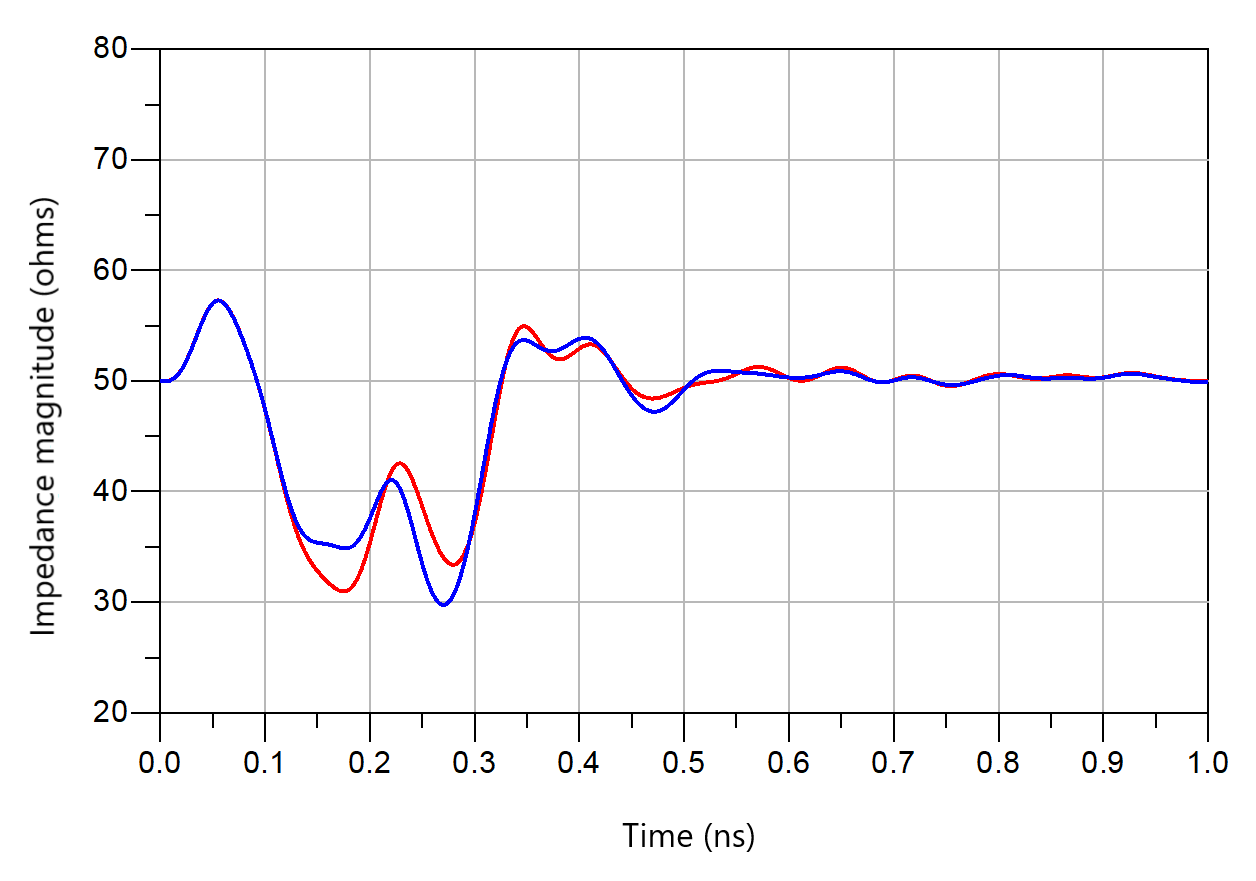
Figure 6 shows the HFSS configuration used to perform a differential S-parameter simulation. This simulation project includes the same connectors used in the previous single-ended S-parameter simulation. Like the previous simulation, the substrate used for the PCBs is 15-mil Rogers RO4350B (microstrip configuration) on top of a single layer of the same substrate set to 134 mils. Figure 7 shows the simulated return loss and insertion loss up to 5 GHz. Again, the insertion loss remains within 2 dB up to 5 GHz. Figure 8 shows the location of the reference plane used for the simulation.
 Figure 6. HFSS configuration used to perform a differential S-parameter simulation. Again, the HMK200MDA3A97E5C male connector is attached to the HMK200FDA3A98E5C2 female connector. Notice the differential traces on the PCB.

 Figure 8. The ports were de-embedded to the location shown by the red line. Again, the pins with the black dots (and the pins not attached to the PCB) are assigned the “non-model” property using the “Dynamic Region Selection” feature.
Figure 9 shows the simulated TDR of the differential configuration. Again, a step input with a 25-ps rise time is used. The red trace represents the reflection from the PCB attached to the HMK200MDA3A97E5C male connector, while the blue trace corresponds to the reflection from the PCB attached to the HMK200FDA3A98E5C2 female connector.

For further reference, Figure 10 shows a closer look at the PCB configuration used for the differential S-parameter simulation. As mentioned earlier, the substrate used here is 15-mil Rogers RO4350B on top of an inner layer of RO4350B substrate set to 134 mils. Note that the 15-mil Rogers RO4350B layer is actually shown on the bottom of Figure 10.
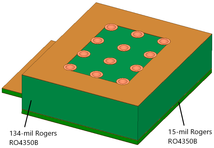
Figure 11 shows a closer look at the connectors used in the simulation. Note that only the shaded pins (12 pins total) are included in the simulation, while the rest are assigned the “non-model” property using the “Dynamic Region Selection” feature. The outer ring of pins are sufficient for carrying ground current. The total pin selection represents a quasi-stripline or quasi-coaxial section.

Simulating Crosstalk
Crosstalk was mentioned earlier as a parameter that may not be predicted correctly unless the PCB and connector are simulated together. The Modelithics 3D models for IEH connectors make it possible to simulate crosstalk. Figure 12 shows an HFSS configuration used to perform a single-ended crosstalk simulation. Again, this simulation project includes the HMK200MDA3A97E5C male connector attached to the HMK200FDA3A98E5C2 female connector. PCBs are again attached to the other side of both connectors. The substrate stackup is the same as before. Figure 13 shows the simulated far-end crosstalk (FEXT) and near-end crosstalk (NEXT).
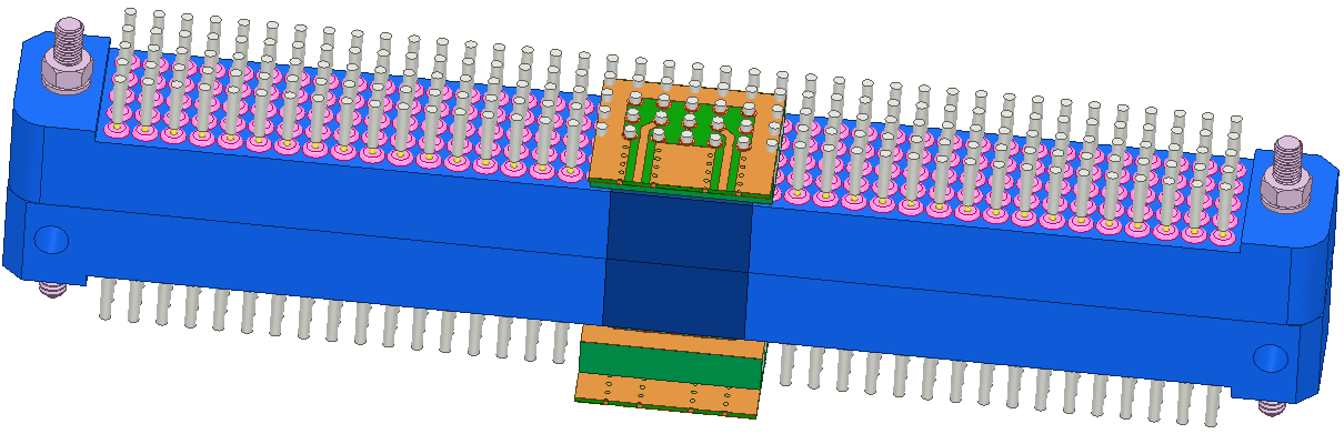
 Figure 13. Shown are the simulated FEXT and NEXT crosstalk results of the single-ended configuration.Figure 14 shows an HFSS configuration used to perform a differential crosstalk simulation. Again, the same connectors and PCB substrates are used for this simulation. Figure 15 shows the simulated FEXT and NEXT.
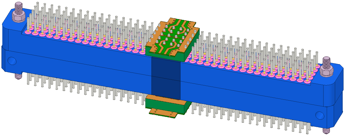 Figure 14. HFSS configuration used to perform a differential crosstalk simulation.
 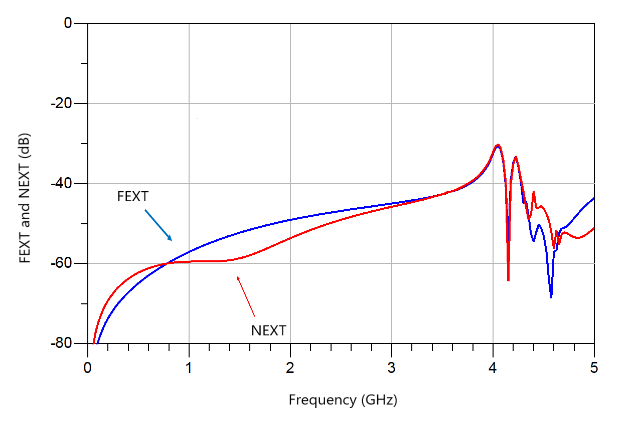 Figure 15. Shown are the simulated FEXT (blue) and NEXT (red) crosstalk results of the differential configuration.
Digital Signal Analysis
A digital signal analysis is the final analysis shown here. For this analysis, the same differential configuration shown in Figure 6 is used. The simulation is performed with pseudorandom bit sequences with a rise time of 50 ps. Figure 16 shows the simulated eye diagrams with data rates of 1, 2.5, and 4 Gb/s. Although some noise is present at 1 and 2.5 Gb/s, the eye opening is wide and maintains a reasonably square shape. At 4 Gb/s, jitter starts to narrow the eye opening, and noise distorting the shape. Hence, operating at 4 Gb/s without mitigation may increase the bit error rate (BER).
 Figure 16. Simulated eye diagrams with data rates of 1, 2.5, and 4 Gb/s.
Figure 16. Simulated eye diagrams with data rates of 1, 2.5, and 4 Gb/s.
Conclusion
For today’s demanding requirements, quality connector models are essential for designers interested in simulating real-life performance. This paper demonstrates some of the simulation capabilities offered by Modelithics 3D models for IEH hyperboloid connector products, including single-ended and differential S-parameters, crosstalk, and digital signal analysis. Designers incorporating PCB connectors into their designs may want to consider these models.
REFERENCES
1. J. Love, “High Bandwidth Connectors: Sorting Out What Matters,” Signal Integrity Journal, 2022, pp 14-16.
2. C. DeMartino, D. Barry, “3D Connector Models Dynamically Reduce Simulation Time,” Modelithics Model Rap blog, January 2023.