
Signal and power integrity (SI/PI) simulations, measurements, and analysis usually live in two different worlds, but occasionally these worlds collide. One such collision occurs when we refer to characteristic impedance, Z0. Traditionally the PI world lives in the frequency domain while the SI world lives in the time domain.
When designing a power distribution network (PDN) in the PI world, we are mostly interested in engineering a flat impedance below a target impedance from DC to the highest frequency components of the transient current. Practically this is achieved with a network of capacitors with different values connected to the respective power planes as shown in Fig. 1.
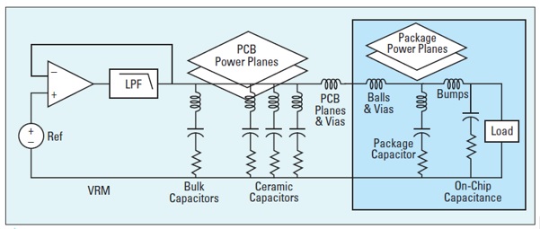
Fig. 1 A simplified model of a typical PDN courtesy [1].
In the real world, there is no such thing as an ideal capacitor. There are always parasitic elements known as equivalent series inductance (ESL) and equivalent series resistance (ESR). Physical characteristics of the PCB, like component mounting inductance, plane spreading inductance, via and BGA ball inductance, along with voltage regulator module (VRM) characteristics also contribute to the impedance profile. When connected together, the interaction of capacitors and parasitic inductance and resistance create a transfer impedance profile with resonant peaks and anti-resonant nulls as shown in Fig. 2.
The transfer impedance between the VRM and the load is calculated and plotted in the frequency domain with a log-log scale. The resulted impedance curve is then compared to the target impedance (Ztarget), which is estimated based on the allowed noise ripple and maximum transient current. The flat target impedance is frequency independent in the analysis.
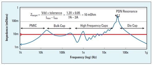
Fig. 2 Impedance profile of the PDN as viewed from the pads on the die power rail courtesy [1].
Resonant peaks are due to ESL of one capacitor connected in parallel with another capacitor. Anti-resonant nulls are due to the series combination of ESR, ESL, and C for each capacitor. Different capacitor values will have anti-resonant nulls at different frequencies.
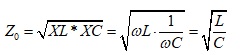
But in the PI world, there is a rarely talked about characteristic impedance, Z0. In this case, it refers to the geometric average of the reactive impedance of a capacitor (XC) and reactive impedance of an inductor (XL).
Equation 1
At resonance, XL and XC intersect at the characteristic impedance and are equal as shown in Fig. 3.
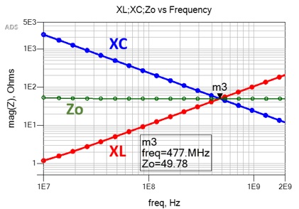
Fig. 3 Inductive and capacitive reactance plot of ideal inductor and capacitor versus frequency. At resonance, XL and XC are equal and intersect at the characteristic impedance, Z0. Simulated with Pathwave ADS [6].
This is a very important observation, and it is where the SI/PI worlds collide.
In the SI world, characteristic impedance, Z0 refers to the instantaneous ratio of the voltage to current of a wave front traveling along a uniform transmission line without reflections. For an infinitely long uniform transmission line, Z0 equals the input impedance.
The characteristic impedance of a lossy transmission line is defined as:
Equation 2
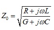
Where R is resistance per unit length; G is conductance per unit length; L is inductance per unit length; and C is capacitance per unit length. For a lossless uniform transmission line, R and G are assumed to be zero and thus the characteristic impedance is reduced to:
Equation 3

Time Domain Reflectometer
In the SI world, we usually use a time domain reflectometer (TDR) to measure characteristic impedance, but more often than not, the measured impedance we get is not what we predicted with a 2D field solver. Many 2D field solvers used by most PCB FAB shops only calculate the lossless characteristic impedance of the cross-sectional geometry at a single frequency, defined by the dielectric constant (Dk). It has no input for conductor resistivity, dielectric loss, or how long the conductor(s) is.
So the issue is: we design the stackup, then do our SI modeling analysis based on stackup parameters and matching characteristic impedance. But the PCB FAB shop will often adjust the line width(s), over and above normal process variation, so that when measured, the impedance will fall within the specified tolerance, usually +/-10 percent.
Part of the problem lies with the method used to take the measurements. Most PCB FAB shops follow IPC-TM-650 Test Methods Manual [2]. But it has limitations because Z0 measured is derived and cannot be directly measured. The reason is the measurements include resistive and dielectric losses, up to the point where the measurement takes place along the TDR plot.
Resistive loss often results in a slow monotonic rise in the impedance profile, shown in the example TDR plot of Fig. 4. IPC-TM-650 specifies a measurement zone between 30-70 percent to avoid probing induced ringing affecting the measurements. Most PCB FAB shops will measure an average impedance over this range, usually in the center region.
Depending on the linewidth, thickness and dielectric dissipation factor (Df), the slope of the monotonic rise will vary.
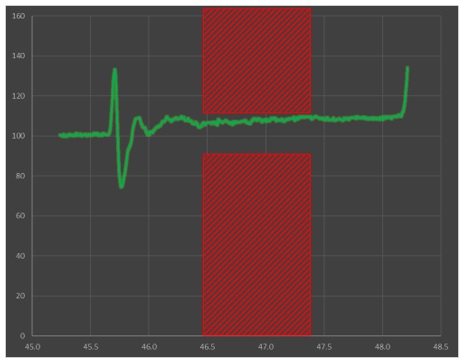
Fig. 4 Example TDR plot showing slow monotonic rise in impedance due to resistive losses and IPC-TM-650 measurement zone.
The problem is that the IPC-TM-650 test method was last updated back in 2004, when higher dielectric loss, along with wider line widths and thicker copper weights, were used more often. A higher Df tends to compensate for resistive loss by flattening the slope as shown in Fig. 5.
On the bottom left is a simulated TDR plot using a high loss dielectric with Df = 0.024. The right side has the exact same geometry properties except Df = 0.004. The average impedance, when measured at the 50 percent point, is 49.8 Ohms on the left side vs. 51.4 Ohms on the right side. We also confirm flatter slope for high loss material.
The actual characteristic impedance predicted by a Polar SI9000 2D field solver [5] in Fig. 5 is 49 Ohms. For higher loss material, measuring within the measurement zone would pass without any issues. But for lower loss material, the resistive loss dominates and measuring within the measurement zone will give ~5 percent higher impedance reading compared to the higher loss material. The correct measurement point for Z0 is, in fact, the initial dip, equivalent to the field solver prediction. Depending on the tolerance specified, this may affect yield and cost.
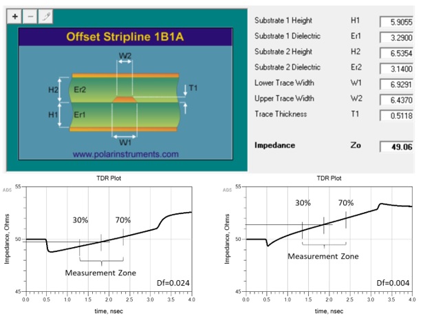
Fig. 5 Characteristic impedance prediction by Polar SI9000 2D field solver [5] (top). Simulated 2 inch TDR plots using a high loss dielectric (bottom left) vs. low loss dielectric with exactly the same geometry (bottm right). A higher Df compensates for higher resistive loss thereby flattening the curve. Simulated with Pathwave ADS [6].
Today, with the push to low loss dielectric and finer line widths with thinner copper weights, measuring the true transmission line characteristic impedance using a TDR becomes more challenging. This is even more so when measuring differential impedance, because a change in line width space geometry can have a more profound effect on measured differential impedance.
Using the first article build of a new design, as an example, let’s assume the correct characteristic impedance, when measured at the beginning of the slow monotonic rise of a TDR plot, is on the high end of nominal +10 percent tolerance. Let’s say it’s 54 Ohms. But because of the low loss dielectric and high resistive loss, the TDR measurement at the midpoint is now reading 5% higher at 57 Ohms. This would imply the impedance is now out of spec over nominal and the board would be scrapped.
The PCB fab shop will then go back and adjust the linewidth accordingly for the next build to bring the measurement within range to their measurement set up. Doing this effectively lowers the true nominal characteristic impedance!
If subsequent manufacturing variations pushes the measured impedance within the measurement zone on the low end of the -10 percent tolerance, say 44 Ohms, then the true characteristic impedance, if measured at the initial dip, will be 5 percent lower at 42 Ohms and be out of spec. But the board will pass because it was measured following IPC-TM-650 test method.
2-port Shunt Measurement
But what if there were another way? What if we could borrow impedance measuring techniques from the PI world to determine the true transmission line characteristic impedance in the SI world? Well there is. Enter the 2-port shunt measurement technique.
For example, in the PI world, to measure ESL and ESR of a chip capacitor, of a device under test (DUT), a 2-port shunt measurement is often used. It is much like the 4-point Kelvin measurement technique used to measure very low DC resistance.
The 2-port shunt measurement is usually done with a 2-port vector network analyzer (VNA). Port 1 of the VNA sends out a calibrated signal, and port 2 measures the voltage signal across the DUT. Often an isolation transformer is also used to break the inherent ground loop when measuring ultra-low impedances [3].
Once the measurements have been completed and S-parameters saved in touchstone format, further analysis can be done in your favorite SPICE simulator. Fig. 6 is a generic schematic using popular Pathwave ADS [5] that can be used for 2-port shunt analysis.
When port 1 and port 2 are connected to port 1 of the DUT and port 2 of the DUT is grounded, the impedance of the DUT can be determined by [3];
Equation 4
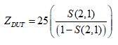
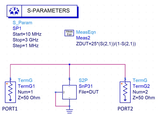
Fig. 6 Generic Pathwave ADS [6] schematic used for 2-port shunt analysis on a S2P file for DUT.
If we replace the DUT in Figure 6 with a capacitor and inductor, we get an impedance plot shown in Fig. 7. As we saw earlier, when we take the geometric average of the inductive and capacitive reactance using Equation 1, we get the characteristic impedance. If we apply Equation 4 to the results of a 2-port shunt measurements of a capacitor and inductor, we get exactly the same results as shown in the top of Fig. 7.
When we replace the capacitor and inductor with a S-parameter file of a transmission line model from Fig. 5, we get the plot shown at the bottom of Fig. 7. Except for the resonant nulls and peaks, up to a certain frequency, the impedance of a transmission line looks like the impedance of a capacitor when the far-end is open, and looks like the impedance of an inductor when the far-end is shorted. And because of that, this is where the two worlds collide!
If we take the geometric average of the impedance when the far-end is open (Zopen) or shorted (Zshort), we get the characteristic impedance at that frequency. We note where the red and blue impedance lines first intersect, is exactly the geometric average characteristic impedance at that frequency.
Also worth noting, the lines intersect at half of the frequency between the peaks and valleys at higher frequencies as well.
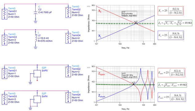
Figure 7 Impedance of inductive and capacitive reactance vs. frequency (top) and impedance of a transmission line vs. frequency (bottom) when the far-end is open (solid red) compared to when the far-end is shorted (solid blue). The intersection of the red and blue lines is exactly the characteristic impedance. Simulated with Pathwave ADS [5].