
Launch Point Extrapolation helps measure characteristic impedance on fine line PCB traces.
Sometimes your intuition may lead you astray… I recently experienced this when two newly fitted thermostatic shower units ran either scalding hot or freezing cold – and nowhere in between – same symptoms – and two identical units. Two plumbers scratched their heads to no avail and reluctantly it looked like needing to rip out the newly tiled in units as they had tried repeatedly to calibrate the min and max temperature with no success. Some months later still with no resolution – a third plumber took a look. He took a different approach. “First – let me look at your boiler”… aha… he noted – you have a reverse boiler. Most boilers have a heating coil to heat a tank of water for use in the shower – this boiler looks like one of those – but in this case the tank is filled with anti-freeze solution and is used as a heat store to heat a coil of mains pressure water. Immediately a light came on in his head – the installers had fitted shower mixers designed for high pressure cold, and low pressure hot water – with a venturi device used cleverly to boost the hot water pressure as the high pressure cold mixed in. I guess the moral of this story is that no matter how well you think you understand a system – external factors can often ruin your intuition and you need to look at the bigger picture – which leads me on to a more relevant topic for Si engineers and how PCB transmission line characteristic impedance is measured especially when the traces are very fine.
But first a confession, in my day job as a supplier of tools for modelling and measuring PCB transmission line impedance – it is easy to get lazy with terminology – Dr Eric Bogatin recently reminded me that the term impedance is used in a variety of ways. And the terminology is important to avoid misunderstanding. When I refer to modelling impedance or measuring impedance it is almost always in the sense of modelling the characteristic impedance of the PCB transmission line. This in contrast to measuring the input impedance of a PCB transmission line. Characteristic impedance of a uniform line is an inherent property of the line itself and for a uniform line – looks the same wherever it is measured. It is broadly independent of frequency and has the fortunate property of looking like a resistance, so that with the correct source and load termination a line can be made to look infinitely long. Designers new to high speed work may confuse characteristic impedance with input impedance of a section of line – which most definitely changes with frequency.
Measuring the characteristic impedance of most PCB transmission lines is straightforward and is usually achieved with a TDR – but it is important to “see” the characteristic impedance free from the impact of the interconnect from the test system, or effects from the end of the line under test. For this reason, many fabricators prefer to use a test coupon for measuring the line characteristic impedance as it can be long enough to allow the TDR to look at the reflection on the undisturbed part of the trace, i.e. the portion beyond the settling of the interconnect aberrations from the test probe, and also away from the rise caused by the open circuit reflection at the end of the coupon.
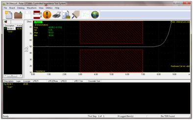
Fig 1 TDR transmission line trace where resistive effects
are small enough to ignore
What has launch point extrapolation (LPE) got to do with this – you may be asking? Well, whilst PCB traces were fairly wide a few mils or hundreds of microns, it was pretty easy to look at the PCB trace and get a flat response to measure the reflection coefficient and either work the math – or have the test system work the math for you and measure the characteristic impedance. If the reflected signal rose or fell along the test transmission line this could safely be deduced as being down to etch taper along the line – and multiple microsections would confirm. But now line widths can be narrower, just a few mils (well below 100 microns) and copper weights are lower, and this can lead to the DC resistance of the transmission line exhibiting itself as a fairly linear upward slope on the TDR trace. If you are unsure if the slope is resistance dependant – you can measure an appropriate coupon from either end and check the slope goes upwards over time regardless of the end of the line being tested. (If the slope goes up from one end and down from the other – it is highly likely that the etching is uneven and the line is narrower at one end than the other – a cross section can confirm).
Once you have confirmed the trace slope results from resistive effects – the challenge is then to remove the resistive element from the measurement – as to get a good reflection free launch into the trace the signal needs be launched with an impedance that matches the instantaneous impedance of the trace. Also when modelling the trace with a 2d field solver the Zo calculated will be the instantaneous impedance. Launch point extrapolation is a technique proposed to more accurately measure the characteristic impedance on finer geometry transmission line PCB traces by many OEMs and the IPC.
Here is an example (Fig 2) showing a typical TDR measurement of impedance on a fine geometry / thin copper trace. Fabricators have become accustomed to taking the average of the undisturbed region of the trace to indicate the instantaneous impedance at any point along the PCB transmission line. But the slope superimposed on the trace begs the question – at which point is the instantaneous impedance the “characteristic impedance?”
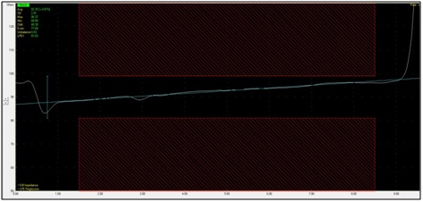
Fig 2 – TDR trace showing resistive loss effects
Figure 3 highlights this further – should you interpret the value – at the start, middle or end of the trace or an average of all three?
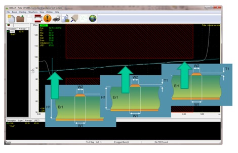
Fig 3 – TDR trace showing resistive loss effects. Where should Zo be
measured?
Thinking about this – the characteristic impedance of a lossless line is usually approximated as in Figure 4
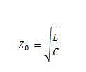
Fig 4 Simplified Characteristic impedance equation
However on fine lines – observed by a TDR – the resistive components come into play

Fig 4 Characteristic impedance equation
So the more complete equation shows R and G, these are dimensional characteristics and will be proportional to length. When solving the line impedance with a 2d field solver the characteristic impedance is computed for a zero length cross section. During measurement of fine line traces the R shows as an upward slope of the trace, and the conductance is still small enough to be ignored. To remove the “R” from the measurement, Launch Point Extrapolation is proposed by a number of OEMs and the IPC in IPC-TM-650 test methods standard, this is a simple line fit projecting back to an imaginary point at the launch of the TDR pulse into the line under test. The impedance at this point is impossible to interpret on a TDR as when you look at the point where the trace starts you will find the TDR reflection perturbed by launch aberrations, and the settling of the pulse amplitude on the line under test. LPE simply fits a line on the unperturbed area of the test vehicle and projects it back to the start of the trace or “launch point” and where this line intersects the point at the end of the probe and the start of the trace – denotes the characteristic impedance.
What happens if you don’t use LPE when measuring fine line traces? If you go back to the shower story at the start of this article – you need to think about some of the facts you are ignoring or unaware of. For example, some fabricators may pick a point in the middle of the trace or take the average value as the characteristic impedance. When they try to correlate they find the measured characteristic impedance is a couple of ohms higher than predicted – and by jumping to the wrong conclusion they may “blame” the accuracy of the dielectric constant of the base material (erroneously) as the cause of the lack of correlation. Next they may use a solver to reverse goal seek the “effective” dielectric constant – when they should be seeking the source of measurement and not modelling inaccuracy. A clue to this happening (and I have witnessed this on several occasions) is a fabricator saying the effective dielectric constant of the glass / resin composite is less than that of the resin. In extreme cases I have seen a fabricator say the Er is less than 2.0 on an innerlayer of FR4 construction. (2.0 would represent pure PTFE!) when the glass in FR4 is around Dk of 6 and the Epoxy around Dk of 3 so a quick common sense sanity check would say this assumption is flawed. I always question fabricators who goal seek Dk in this way – as other variables (dielectric separation and line width) have a first order impact on characteristic impedance, Dk has a 1/root influence – so simply surfing this number around can easily lead to wrong conclusions.
In summary – when measuring characteristic impedance on fine line traces, it is important to use a long enough test vehicle to enable a good line fit away from TDR pulse settling and launch aberrations so as you can apply launch point extrapolation. Correlation studies with 2d field solvers should then be based on correlating the field solver value with that measured by the Zo projected at the start of the test coupon by the LPE line fit.
BIOGRAPHY
Martyn Gaudion is Managing Director of Polar Instruments Ltd. He began his career at Tektronix in the early 1980’s where he was responsible for test engineering on high bandwidth portable oscilloscopes. During his time at Tektronix he gained widespread experience of PCBA production and was extensively involved with introduction of surface mount technology. Gaudion joined Polar in 1990 where he was responsible for the design and development of the Toneohm 950, Polar’s multilayer PCB short circuit locator. He became marketing manager at Polar during 1997 as the market for controlled impedance test became a major section of Polar’s product range, appointed Sales & Marketing director in January 2001, appointed CEO in January 2010, Gaudion also writes occasional articles for a number of PCB industry publications and regularly contributes to IPC High Speed High Frequency standards development activities. Gaudion is a Chartered company director and a Fellow of the London based IoD (Institute of Directors). In 2016 appointed vice chairman of the European Institute of Printed Circuits (EIPC).