
You would think that interconnect design for rf applications and high-speed digital applications would be very similar. After all, the upper frequency range of the applications are similar. Figure 1 shows the frequency of various rf and microwave specs and the bandwidth corresponding to different high=speed digital serial link communications lines.
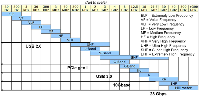
Figure 1. Overlap of rf and high-speed digital spectral ranges.
For example, 10Gbase Ethernet, at 10 Gbps, has frequency components into the 25 GHz regime, where K and Ka band radars operate. Aren’t the problems and design solutions rf engineers use the same as those of high-speed digital designers, if the frequency range of interest is the same?
The surprising answer is no. These applications, though sharing an upper frequency range, require very different design principles and is the main reason why there is usually a disconnect when an rf engineer tries to design a high-speed digital product and vis versa.
The differences start right in the way an rf engineer views the world compared to a high speed digital engineer. The rf engineer lives in the frequency domain. Their intuition is rooted in the frequency domain. How they approach signals and interconnects is all about the frequency domain perspective.
The high speed digital engineer, in contrast, lives in the time domain. Digital performance is measured in the time domain; signals exist in the time domain. Their intuition about the signals and how they interact with the interconnect is rooted in the time domain.
There are four other important differences in the design principles for rf and high-speed digital applications which make the best design practices for one world, almost the opposite for the other. Let’s take a look at some of these differences.
Bandwidth of the signals
The bandwidth of a signal is the frequency range for the important information content of the signal. Typically, in rf applications, there is a carrier frequency with some modulation. The bandwidth of the rf signal is narrow, maybe only a few MHz, depending on the application, though the carrier may be at 2.5 GHz, as in 802.11abg wifi.
In high-speed digital applications, there is a highest frequency component in the signal, depending on the rise time of the signal, but the important frequency components extend all the way down to DC. This makes the bandwidth of digital signals very large. This comparison is illustrated in Figure 2.
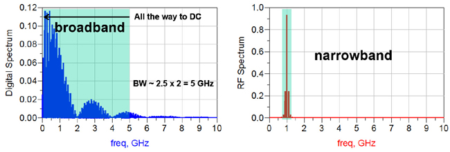
Figure 2. Comparison of the spectrum and bandwidth of 2 Gbps digital and 1 GHz carrier rf signals.
The Very Idea of Impedance
Impedance is arguably the most important metric of an interconnect for any application. The impedance properties of an interconnect dominate the performance of the interconnect in all high frequency applications. Yet, it is also one of the most confusing topics in discussions between an rf and high speed digital engineer. This is because they each use the same term, but are implying a different type of impedance.
Using the term “impedance” alone, is ambiguous. There are many different types of impedance and each one has a very different, specific definition. When an rf engineer refers to the impedance of an interconnect, they usually mean, “the input impedance in the frequency domain” of the interconnect. When a high speed digital designer refers to the impedance of an interconnect, they usually mean, “the characteristic impedance” of the interconnect, which, for a uniform transmission line, is the “instantaneous impedance” the signal sees as it propagates down the transmission line.
For the rf design, they care about the impedance of the interconnect at a specific frequency, within a narrow frequency range. They can engineer the input impedance of the interconnect by adjusting its length, its shape and even adding stubs connected, or adjacent. The input impedance is important only at the carrier frequency. What happens at other frequencies is generally irrelevant.
The digital designer cares about the impedance of the line from DC to a very high frequency. The important term is the instantaneous impedance the signal sees as it propagates each step along the interconnect. The important design guideline is to keep this impedance constant throughout the line. This means controlled cross section and managing the impedance at the end, usually by adding a resistor to fake the signal into seeing no change in instantaneous impedance. This distinction is illustrated on Figure 3.

Figure 3. Input impedance to an rf designer and instantaneous impedance to a high speed digital designer.
Stubs
Mention the word stub around an rf designer and you will get a happy smile. A stub is an incredibly powerful design feature to tailor the impedance of the line to exactly what the designer wants.
Mention the word stub around a digital designer and you will get a scared, frantic look in their eyes. They want to do everything they can to avoid stubs as these features will set the fundamental limit to how high a data rate their channel will support.
Capacitors
As a last example, consider how capacitors are used in these two worlds. Every type of product will use capacitors, sometimes with as many as 10-500 individual ones in the product. Yet, the applications are sometimes different and their requirements for the capacitors are different. Figure 4 shows an example of an rf radio product with more than 50 capacitors.

Figure 4. Example of a rf radio product with more than 50 capacitors.
An rf engineer may use a capacitor as a filter or as part of an oscillator circuit. In these applications, the most important property of the capacitor is its ESR. This contributes to the q-factor of the circuit, the sharpness of the resonance or the edge of the filter response. For rf applications, high q-factor is high value and capacitors should have as low an ESR as possible.
To a high speed digital designer, a common application for capacitors is to provide low impedance in the power distribution network (PDN). Here, the important metric is also what happens at resonances, usually parallel resonances which produce peak impedances. But, what is important to the digital designer is to engineer very poor resonances, to damp out the resonances. The worst feature possible is to have a high q-factor resonance with a large peak impedance,
A digital designer will do everything they can to damp out resonances. This is sometimes accomplished using high ESR capacitors.
These are just a few examples of how rf engineering is different from high speed digital engineering. The next time you are in discussion with your opposite counterpart, be aware of your different world views and appreciate each other in context.