
We can see this more clearly if we replot Fig. 7 bottom using a linear scale for the x-axis, as shown in Fig. 8. This is a very powerful observation. What this means is that when we measure the impedance half way between a peak and adjacent valley, of either the red or blue plot, it is the characteristic impedance of the transmission line at that frequency.
Thus, only an open or shorted end measurement is all that is needed to determine the characteristic impedance. For example, if we look at the red curve alone, then measure the first resonant null (m14) and adjacent peak (m15), the characteristic impedance (mag(Zopen) is measured exactly at one half the frequency between the two (m16).
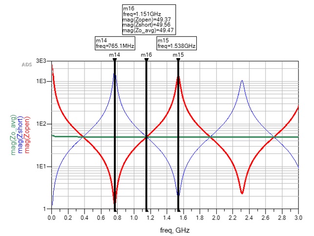
Figure 8 Impedance of a transmission line vs. frequency on a linear scale when the far-end is open (solid red) compared to when the far-end is shorted (solid blue). The intersection of the red and blue lines half way between respective peaks and valleys is the characteristic impedance. Simulated with Pathwave ADS [6].
The first resonant red null and blue peak represent the quarter-wave resonant frequency due to open and shorted end. Each respective red null and blue peak following are the odd harmonics of the first quarter-wave resonant frequency.
Knowing this, we can now determine the phase or time delay (TD) of the transmission line as being one quarter of the period of the resonant frequency (f0).
Equation 5

Because resonant nulls and peaks occur at the resonant frequency, we can also determine the effective dielectric constant (Dkeff). Given the speed of light (c) = 11.8 in. per nanosecond, the length of the transmission line (len) in in. and quarter-wave resonant frequency (f0), Dkeff can be determined by:
Equation 6

CMP28 Case Study

Figure 9 Photo of a portion of CMP-28 test platform courtesy of Wildriver Technology [8] used for measurement validation.
To test the accuracy of this method, measured data from a CMP28 test platform, shown in Fig. 9, was used for measurement validation. S-parameter (s2p) files from 2 inch and 8 inch single-ended stripline traces were provided as part of CMP-28 design kit courtesy of Wildriver Technologies [8]. The 6-inch transmission line segment S-parameter data was de-embedded courtesy of AtaiTec Corporation [9].
The characteristic impedance, based on trace geometry and stackup parameters, was modeled in Polar SI9000 [5]. Using Dk from data sheet tables @ 10GHz, and correcting for conductor roughness [10], the characteristic impedance predicted was 49.66 Ohms, as shown in Fig. 10.
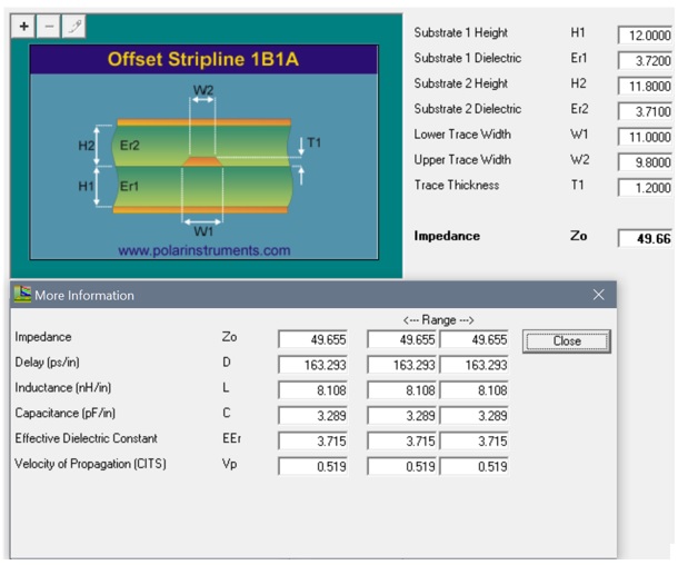
Figure 10 Polar SI9000 field-solver [5] characteristic impedance prediction of CMP28 trace geometry.
Touchstone S-parameter DUT files were connected with far-end open, shorted, and terminated as shown in Fig. 11. The TDR plot, with far-end terminated, shows an impedance of 50.57 Ohms, when measured at the initial peak. Then it takes an immediate dip to approximately 50 Ohms before continuing with a slow monotonic rise with some ripples. If the DUT was a uniform trace, with connector discontinuity de-embedded, we would not see the initial peak followed by the dip. This signature strongly suggests that the DUT is not uniform and thus it is very difficult to determine the actual characteristic impedance using IPC-TM-650 test method alone.
But only after taking 2-port shunt measurements can we confirm the true characteristic impedance. As shown, Zoavg is 50.68 Ohms where the red and blue curves cross at 122.5 MHz, and confirms the true measurement point in the TDR plot is the initial peak. Both are about 1 Ohm higher compared with 2-D field solver results in Fig. 10.
If the length of the transmission line simulated above is 6 in. and f0 =248.2 MHz, then TD = 1 ns and Dkeff = 3.92, using Equation 5 and Equation 6 respectively.
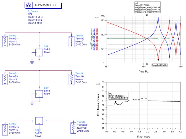
Figure 11 Measured results from a CMP28 test platform design kit, courtesy of Wildriver Technology [8].
But wait a minute. Why is Dkeff is higher than what was used in the 2-D field solver in Fig. 10?
One reason is due to process variation of the material and fabrication. The actual Dkeff is determined by the final thickness of dielectric and the roughness of the copper, which also increases inductance affecting TD [10] [11]. But the main reason is Dk is frequency dependent and the value used in the field solver was at 10 GHz, based on laminate supplier’s Dk/Df tables.
Since TD, ultimately determines Dkeff, it does not represent the intrinsic property of the dielectric material. Because Dkeff varies with frequency, it was calculated at the first resonant null of 248.2 MHz, which is at a much lower frequency for Dk than the frequency originally used to select Dk in the field solver.
As can be seen in Fig. 12, a simulated vs. measured 2-port shunt frequency plot, with far-end open and shorted, we get exactly the same information, compared to the traditional method used to validate characteristic impedance and Dkeff.
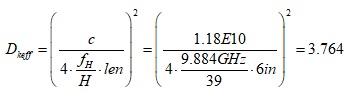
If we measure the 39th odd harmonic frequency (H) at 9.884GHz for the resonant null closest to 10GHz, equating to the value of Dk used in Polar Si9000 2D field solver, Dkeff can be calculated with Equation 7:
Equation 7
The bottom right plot of Fig. 12, shows Dkeff simulated (blue) vs. measured (red). As we can see, the measured Dkeff at 248.7 MHz is 3.94; pretty much agreeing with our earlier calculation of 3.92 using Equation 6. Furthermore, when we compare Dkeff = 3.76 at 9.884 GHz, it agrees with our calculation for the 39th harmonic frequency from Equation 7. The reason there is still a slight difference in Dkeff is because the added delay due to inductance due to roughness [11] was not factored into the simulated model.
The bottom left is a TDR plot that shows measured impedance (red) vs. simulated (blue) over time. The marker at the beginning of the initial dip (m6) represents the characteristic impedance with highest frequency harmonics included in the incident step edge of TDR waveform. The marker at the end (m16) represents the impedance at twice the TD with high frequency harmonics attenuated due to dispersion of the lossy dielectric and resistance of trace length.
When we measure Zoavg_meas impedance of DUT at 9.884GHz, at the top plot of Fig. 12, it agrees pretty well with the simulated and measured TDR plot at the initial step.
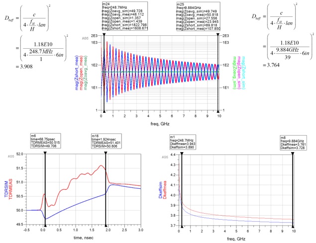
Fig. 12 Comparison of PI world 2-port shunt measurement results for transmission line characteristic impedance and Dkeff compared to traditional SI world measurement results. Top plot is the 2-port shunt simulated vs. DUT impedance measurements at the fundamental and 39th harmonic frequencies. Bottom left is beginning and end impedance measurements on TDR plot. Bottom right measuring equivalent Dkeff at fundamental and 39th harmonic frequencies.
Summary and Conclusion
Sometimes, when SI and PI worlds collide, we get the best of both worlds. By borrowing a simple 2-port shunt impedance measuring technique from the PI world, we have another tool at our disposal to measure true characteristic impedance, TD, and effective Dk from a uniformly designed transmission line in the SI world. The advantage is, unlike a TDR measurement, measuring true characteristic impedance using 2-port shunt method is not influenced by resistive or dielectric losses.
References
-
L. Smith, S. Sandler, E. Bogatin, “Target Impedance Is Not Enough,” Signal Integrity Journal, Vol. 1, Issue 1, January 2019; URL: https://www.signalintegrityjournal.com/ext/resources/MEDIA-KIT-2019/January-2019-Print-Issue/SIJ-January-2019-Issue_eBook_-V2.pdf
-
IPC-TM-650 Test methods Manual, Number 2.5.5.7, “Characteristic Impedance of Lines on Printed Boards by TDR”, Rev. A, March, 2004
-
I. Novak, J. Millar, “Frequency-Domain Characterization of Power Distribution Networks,” Artech House, 685 Canton St., Norwood, MA, 02062, 2007.
-
Pathwave Advanced Design System (ADS) [computer software], Version 2021, URL: http://www.keysight.com/en/pc-1297113/advanced-design-system-ads?nid=-34346.0&cc=CA&lc=eng
-
Polar Instruments Si9000e [computer software], Version 2018, URL: https://www.polarinstruments.com/index.html
-
Keysight Pathwave Advanced Design System (ADS) [computer software], Version 2021, URL: http://www.keysight.com/en/pc-1297113/advanced-design-system-ads?cc=US&lc=eng.
-
E. Bogatin, “Bogatin’s Practical Guide to Transmission Line Design and Characterization for Signal Integrity”, Artech House, 685 Canton St., Norwood, MA, 02062, 2020
-
Wild River Technology LLC 8311 SW Charlotte Drive Beaverton, OR 97007. URL: https://wildrivertech.com/
-
AtaiTec Corporation, URL: http://ataitec.com/products/isd/
-
B. Simonovich, "A Practical Method to Model Effective Permittivity and Phase Delay Due to Conductor Surface Roughness", DesignCon 2017 proceedings, Santa Clara CA.
-
V. Dmitriev-Zdorov, B. Simonovich, I. Kochikov, “A Causal Conductor Roughness Model and its Effect on Transmission Line Characteristics”, DesignCon 2018 proceedings, Santa Clara, CA.
-
I. Novak et al, “Determining PCB Trace Impedance by TDR: Challenges and Possible Solutions”, DesignCon 2013 proceedings, Santa Clara, CA.
-
S. Sandler, “Easy trick to measure plane impedance with VNA”, EDN Asia, 2014, URL: https://archive.ednasia.com/www.ednasia.com/STATIC/PDF/201410/EDNAOL_2014OCT21_TEST_TA_01.pdf%3FSOURCES=DOWNLOAD