
Measured S-parameters and cross-sections of PCB interconnects are used in this paper to identify the parameters of electrical models suitable for statistical analysis of interconnects with manufacturing variations. The constructed models reproduce observed effects of geometry and material properties variations on the loss, delay, and impedance, and they are suitable for yield analysis of interconnects with up to 56 Gbps signals. This is the first attempt to build such models with effects of geometry and material properties variations for PCB interconnects.
The design of predictable PCB interconnects for 56 Gbps PAM-4 links requires an analysis to measurement correlation from 1 to 10 MHz up to at least 40 to 50 GHz. There are three necessary conditions to achieve such correlation.1 First, we need to know the actual PCB interconnect geometry—PCBs are not manufactured as designed. Second, broadband dielectric and conductor roughness models are needed. Third, the accuracy of the analysis software must be systematically validated for this bandwidth.
Theoretically, if all three conditions are satisfied, the models should correlate with the measurements. However, the manufacturing variations may prevent such correlation in case of mass production. Previously, only the effect of variation on impedance or insertion loss was investigated.2-3 In this project, we evaluated effect of geometrical variations on the identified material model parameters and built transmission line models with observed variations of loss, delay, and impedance. The results reported here are the statistical distributions of the strip geometry as well as of parameters of dielectric and conductor roughness models suitable for yield or corner-case analysis of 56 Gbps links.
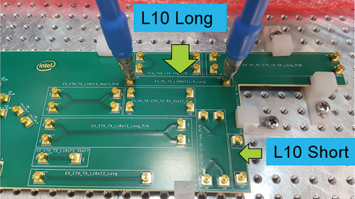
Figure 1. Test coupon view during measurements—only single-ended strip line segments in layer L10 are used in this investigation.
TEST COUPON DESIGN AND MEASUREMENTS
Very low loss dielectric Megtron 7 and smooth HVLP copper were used to meet 56 Gbps channel performance requirements. Short and long segments of striplines with a length difference 1.5 in. were placed on a coupon attached to production boards (see Figure 1). S-parameters of the segments can be used to extract reflection-less GMS-parameters for model identification.4 Three batches of the same board were manufactured. Five boards were manufactured in the first batch (Rev1), 20 boards in the second (Rev2), and 30 in the third (Rev3). A network analyzer with 67 GHz bandwidth and a mechanical 1.85 mm standard calibration kit were selected for all measurements. The measurement setup is shown in Figure 1. S-parameters for the three batches of the test structures were measured. Insertion losses for the short single-ended line segments for all three batches are plotted in Figure 2.

Figure 2a. Quality of measured S-parameters.
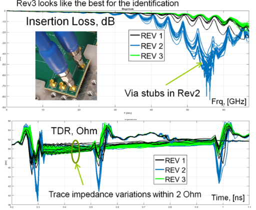
Figure 2b. Insertion loss (right top) for short segments, and TDR (right bottom) for all segments.
The quality of the S-parameters was evaluated with IEEE standardized (P370) metrics of passivity, reciprocity, and overall quality evaluated with the rational approximation (first columns in table of Figure 2). Practically all metrics came out as either good (highlighted in green) or acceptable (highlighted in blue). Structures in the Rev2 batch have stubs on the connector launch vias, whose resonance is visible in the insertion loss plots in Figure 2. It restricted the bandwidth of GMS-parameters. The insertion loss in the structures of Rev3 with back-drilled viaholes was the best. TDRs for all segments were computed from S-parameters and are shown in Figure 2.
We observed an approximate 2Ω variation in the trace impedances and more than 5Ω variation in the connectors-to-launches transitions due to inconsistencies in connector soldering. It further restricted the bandwidth and distorted the GMS-parameters to about 40 GHz. Also, there was about 1Ω systematic offset between impedances of the short and long transmission line segments due to different orientation with respect to laminate fiber.2-3
CROSS-SECTIONING
After the measurements of S-parameters, all test boards were cross-sectioned and geometry variations were observed. Both short and long segments were cross-sectioned, but measurements from the short segments only are used for the material model identification. All measurements of the same dimension are taken at two or three locations as illustrated in Figure 3 and averaged. Results for all samples are shown in Table 1.

Figure 3. Cross-section measurement points.
The major contributor to the conductor losses at lower frequencies and impedance variations is the trace width and thickness. As we can see from the trace width and thickness shown in Table 1, the trace cross-section area can vary between samples by as much as 30 percent. Most of the variations are in the thickness of the trace. Substantial variations of the trace thickness were confirmed by multiple measurements along the trace on the same board—data for one of the samples are in the last row of Table 1. It contributes to the impedance and loss variations and introduces uncertainties into the identification process, especially at lower frequencies.
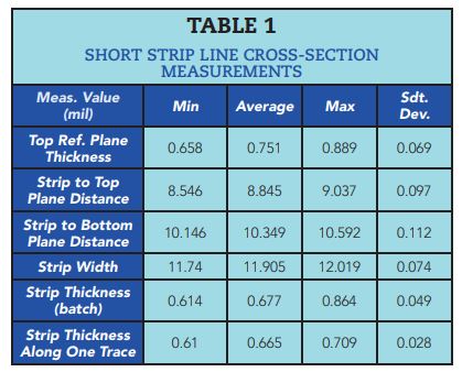
Table 1. Short strip line cross-section measurements.
Considering the thickness of the laminate above and below the strip, the variations are not so large. The material parameters will not be very sensitive to the variations of these parameters. From Figure 3 we can also observe differences in spreading of the fiber bundles. The fiber bundles across the short line cross-section look wider than across the long line cross-section. It was also confirmed by additional cross-sectioning. That difference can explain the systematic 1Ω offset in TDR impedance between the long and short segments.2-3
MATERIAL MODEL IDENTIFICATION
A wideband Debye (aka Djordjevic-Sarkar) model was selected for dielectrics. The model can be uniquely defined with dielectric constant (Dk) and loss tangent (LT) at one frequency point (bandwidth was fixed). A Causal Huray-Bracken model was selected for conductor roughness. The model is uniquely defined by two parameters—surface roughness (SR) and roughness factor (RF).2-3
Identification of Dk, LT, copper relative resistivity (RR, normalized to 1.724e–8Ω*m), SR, and RF is done with generalized modal S-parameters (GMS-parameters).4 We first tried an identification algorithm with the dielectric and conductor loss separation by fitting parameters affecting loss over separate bandwidth1 (for copper resistivity at 10 to 20 MHz, for loss tangent over 0.05 to 1 to 2 GHz, and for roughness model over 3 to 40 GHz). The algorithm did not work well because of an extremely low loss dielectric and large variations of the trace cross-section—it was impossible to separate the losses. Thus, the following modified identification algorithm was used:
1. Fix all cross-section parameters to batch mean values.
2. Identify Dk at 1 GHz first by matching GMS phase delay from 2 to 40 GHz.
3. Identify relative resistivity (RR) with loss tangent LT at 1 GHz simultaneously by matching GMS attenuation from 0.01 to 2 GHz.
4. Identify roughness model parameters SR and RF by matching GMS attenuation from 2 to 25 to 35 GHz.
5. Correct Dk at 1 GHz by matching GMS phase delay from 2 to 40 GHz.
Simbeor SDK with a quasi-static field solver was used to implement and automate the identification process. The identification results for batch Rev3 are in Table 2.
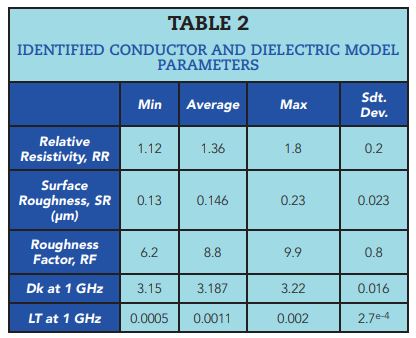
Table 2. Identified conductor and dielectric model parameters.
Correlation of the identified model with the measured GMS-parameters is shown in Figure 4 for Rev3 cases. Spikes in the measured GMS-parameters were attributed to the connector mounting problem.3 With a numerical experiment, we proved that this defect did not affect the identified model parameters. Models with the min and max values in Table 2 produced impedance with min value 47.4Ω, max value 48.41Ω, and average 47.9Ω. The model average impedance correlated well with the impedance observed on TDR for short line segment, and is about 1Ω lower than the impedance of the long line segments.

Figure 4. Measured (red curves) and simulated (blue curves) GMS attenuation and phase delay for 28 cases from Rev3.
An even simpler model with an acceptable accuracy can be constructed by fixing some parameters to the average or reasonable values: LT = 0.001 at 1 GHz, SR = 0.15 um, RR = 1.5.2 Only distributions of Dk and RF are identified in this case with the following outcome: the average value for Dk is 3.188 at 1 GHz with standard deviation 0.015, the average value of RF is 8.13 with the deviation 0.76.
CONCLUSION
The results of the investigation reported in this paper are the first step toward building simple statistical models for the design of predictable interconnects for 56 Gbps PAM4 signals. We observed variations in the geometry and investigated multiple scenarios of the material model parameters identification with statistical variations. In the simplest model, variations in interconnect impedance, losses, and dispersion are reduced to just two model variables with an acceptable accuracy.
REFERENCES
1. M. Marin and Y. Shlepnev, “Systematic Approach to PCB Interconnects Analysis to Measurement Validation,” 2018 IEEE Symposium on EMC and SIPI, 2018.
2. A. Manukovsky and Y. Shlepnev, “Effect of PCB Fabrication Variations on Interconnect Loss, Delay, Impedance & Identified Material Models for 56-Gbps Interconnect Designs,” DesignCon 2019, January 30, 2019.
3. A. Manukovsky and Y. Shlepnev, “Measurement-Assisted Extraction of PCB Interconnect Model Parameters with Fabrication Variations,” IEEE 28th Conference on Electrical Performance of Electronic Packaging and Systems, October 2019.
4. Y. Shlepnev, “Broadband Material Model Identification with GMS-Parameters,” IEEE 24th Conference on Electrical Performance of Electronic Packaging and Systems, 2015.
Article was published in the SIJ January 2020 Print Issue, Technical Feature: Page 20.