
RX ADC-based FFE
After the ADC, the equalization will be performed in the symbol domain if the ADC samples one data point at symbol rate. Compared to analog FFE, the digital FFE is less complicated and more scalable as FFE, mathematically, as it is a convolution between FFE coefficients and sampled incoming data. It can be implemented using a pipeline structure where the throughput can be maintained while the chip area and latency will only grow linearly with the FFE tap length. So, offering FFE with long tap length becomes a viable solution in terms of PPA matrix where it can handle reflections and impedance discontinuities farther away from the main cursor with a reasonable cost.
RX ADC-based DFE
Contrary to ADC-based FFE, ADC-based DFE does not benefit much, relative to the FFE’s case, from this architecture change. The reason is, same as in analog DFE case, the DFE adjustment needs to be computed and applied to the data path, now represented by a FFE-adjusted value, within the one symbol UI. In order to make up the timing requirement for DFE adjustment computation, one possible way is to inject extra delay cycles. ADC-based DFE and associated delay injection have made the DFE less efficient in the PPA matrix.
ADC-specific factors
The performance of the ADC is essential to an ADC-based EQ architecture. Today’s state-of-the-art ADC design will not be able to sample data at line rate and, hence, a bank of ADCs with fixed delay time associated with the ADC’s base clock are used to acquire one sample per UI at line rate. In this process, additional delay is introduced and signal degradation, i.e. capacitance loading and noises, occurs. Therefore, part of the DSP-based EQ performance gain will be consumed by this non-ideality and prolonged latency.
FEC
FEC came into practice with the 25Gbps generation, and it shows its necessity with 50+ Gbps PAM4 operating conditions. At 112Gbps and beyond, FEC is expected to become an essential part of EQ architecture. Our studies [8] show that FEC’s performance depends on SNR at the RX slicer, burst errors caused by ISI and DFE coefficient/adjustment, and modulation schemes. We will further discuss the FEC performance with respect to equalization in the next section.
Equalizer Effectiveness
We conducted a series of PAM4 and PAM8 simulations at 112Gbps using our in-house high-speed link simulation platform [9][10][11] to study the effectiveness of different equalization schemes. The channels under study, where the simulation results were presented in this paper, were drawn from our channel database (profile shown in Table 1). These channels mimic real-world cases where the insertion loss is around 30dB at 28GHz with realistic ILD (insertion loss deviation) and ICR (insertion-loss -crosstalk ratio) characteristics.

The transmitter has the following configuration: Output differential amplitude = 1.0Vp-p(diff), 20%-80% rise/fall time ≈ 6ps, PAM4/8 level mismatch (RLM) = 0.95, return loss ≈ -10dB, TX BUJ (bounded uncorrelated jitter) = 0.04UIp-p, TX DCD (duty cycle distortion) = 0.019 UIp-p, TX RJ (random jitter) = 0.01UIrms, and 4-tap TX EQ with 2 pre-cursor and 1 post-cursor taps.
The receiver is with the following configuration: Return loss ≈ -10dB, RX CTLE AC gain from 0 to 20dB, low-frequency CTLE with gain from 0 to 6 dB, VGA gain from 0 to 20dB, FFE with 3 pre-cursor taps and up to 36 post-cursor taps, DFE with up to 40 taps.
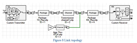
The TX and RX packages have insertion loss of ~2.5dB at 28GHz. The link topology is illustrated in Figure 8.
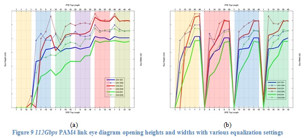
The first experiment was to test the effectiveness of LEQ (linear EQ which consists of TX FIR, RX CTLE and RX FFE) and DFE at various configurations. Because CTLE is usually pre-determined with limited tunability and TX FIR and FFE are mathematically equivalent, we adjusted FFE tap length while fixing the TX FIR setting and sweeping CTLE settings in this experiment. The simulation results are shown in Figure 9 where the eye-opening height (EH) and eye-opening width (EW) at receiver data slicer were measured at BER = 10-4. In order to observe the effectiveness of LEQ/FFE and DFE, we plotted the simulation in two different arrangements. Figure 9(a) plots the EH/EW results sorted first by FFE length and then by DFE length. Figure 9(b) represents the same data, but it is sorted with DFE length first and then FFE length.
A few observations can be noted: FFE’s performance, in terms of EH and EW, scales well with its tap length. It demonstrated a near-monotonic increasing with FFE length, and DFE is seen to provide a supplemental role for these links. On the other hand, DFE’s equalization effectiveness is less linear compared to FFE’s. For these channels, it is seen that a minimum 5-tap FFE is required regardless of DFE length. One of the key differences between FFE and DFE is FFE’s capability to deal with pre-cursor ISI, and these results showed and supported this theory. Further, FFE can also be used to compensate the deficiency and/or PVT variations from CTLE.
The second observation is the optimal EH/EW performance saturated after FFE or DFE lengths reaches about 30 taps. This again coincides with the channel characteristics where the significant reflections and impedance discontinuities of these tests channels are all ended at around 25 to 30UI at 112Gbps with PAM4 modulation scheme.

We also performed the same experiments at 112Gbps with a PAM8 modulation scheme, and the results are shown in Figure 10. The results indicated the same trend regarding LEQ/FFE and DFE equalization effectiveness. PAM8’s results also indicate further degradations of EH/EW compared to PAM4 due to additional modulation levels and modulation ISI. Though PAM8 modulation reduces the symbol rate and consumes less bandwidth, the equalization needs increases compared to PAM4. For instance, for the channel #3, the minimum FFE length increases roughly by 5 taps because PAM8 needs more sophisticated equalizations to achieve the same BER performance.
The next experiment was to check the equalization schemes’ capability in dealing with uncorrelated jitter and noises. Uncorrelated noises are the most challenging factors in HSIO systems as these noises usually cannot be effectively compensated. The most common uncorrelated noise sources include crosstalk, power supply noises, and converted jitter/noise sources (e.g. jitter/noise through a limiting amplifier). It is known that linear equalization schemes, such as TX FIR, RX CTLE, and RX FFE, are not suitable for these uncorrelated noises because they tend to amplify this type of noise. DFE, on the other hand, is more effective in handling the uncorrelated noise because of the decision feedback mechanism where the decision signal is noise free.
We conducted a design of experiments where we controlled the crosstalk amplitude while keeping all other conditions the same. Channel #3 is chosen as it represents the worst-case channel so that the EH/EW results were not saturated. The simulation results represented by EH and EW were shown in Figure 11.
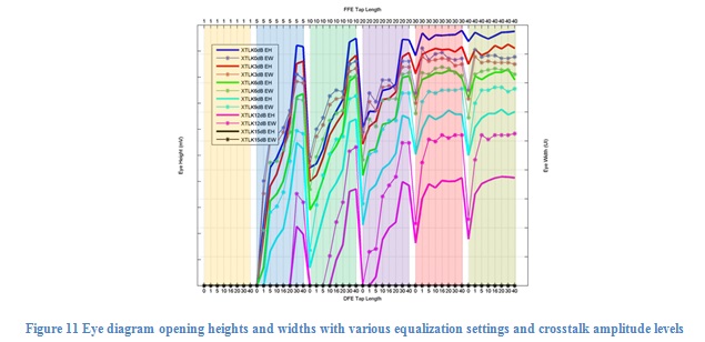
We added a “no DFE” case as a baseline and further extended the DFE length to 40 taps for clearer comparisons. The simulation results provided some interesting insights: First, crosstalk is not directly compensated by FFE, as seen by the EH data points when DFE length is 0. Second, the results showed that FFE and DFE cannot compensate or eliminate crosstalk noise as the EH/EW decreases steadily with the increasing crosstalk amplitude while the FFE’s and DFE’s coefficients were not saturated in the simulations. Third, the effectiveness of DFE, in terms of increasing EH, became more pronounced as the crosstalk amplitude increases. Finally, with crosstalk noise reached 15dB over the original crosstalk noise, the link no longer can achieve BER 10-4 and, hence, EH and EW were both zero.
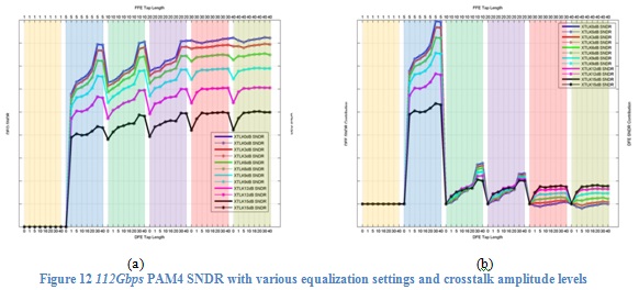
Then we observed the SNDR at the receiver slicer of this experiment shown in Figure 12(a). Compared to Figure 11, the SNDR plot showed the crosstalk effects where the final optimal SNDR, i.e. with maximum FFE and DFE tap length, align nicely with the amount of crosstalk noises in the links. The 15dB crosstalk case, where the link cannot achieve BER 10-4, the SNDR figures can still be extracted at the data slicer of the receiver. We further processed the results by using the no DFE case as a base point and generated the plot shown in Figure 12(b). Figure 12 shows a couple of interesting factors: First, as soon as the minimum amount of FFE or, to be more precisely, linear equalization which covers both the pre-cursor and post-cursor ISI, the DFE’s capability to improve SNDR is significant especially with short FFE length. Then, with full equalization, i.e. with 30 taps of FFE, the DFE will continue to improve SNDR under heavy uncorrelated noisy condition. Finally, it shows that, with regard to uncorrelated noises such as crosstalk, we will only need a few DFE taps to achieve optimal results.

Similar results were observed in the same experiment but with PAM8 modulation scheme and the results are shown in Figure 13. It demonstrated the same trend we saw earlier that PAM8, though running at lower frequency, requires more equalization to achieve its optimal point. Note that, because PAM8’s symbol level separation is smaller than PAM4, the 15dB case failed to work and the RX slicer cannot detect or recover data regardless of the EQ settings. Same as in the PAM4 case, the results also pointed out that a short DFE is needed for compensating uncorrelated noises.
FEC is an essential part of next generation equalization. Our studies [8] indicated that FEC’s performance, i.e. the amount of BER improvement usually in power of 10 scales, depends on a multiple of factors which include FEC schemes, residual noise seen at the receiver, modulation scheme (e.g. NRZ, PAM4, PAM8), coding scheme (e.g. linear coding, gray coding), equalization schemes, and settings. Figure 14 shows the Reed Solomon RS(544, 514, 10) FEC BER gain comparisons between PAM4 and PAM8 modulation schemes.

From Figure 14, we can see that the FEC BER gain degrades from PAM4 to PAM8. The reason is that, in the NRZ scheme, there are only two levels so that there is no further error expansion when the noise occurs in the outer region. In PAM4 or PAM8, noise occuring in both ends of a symbol level will continue to contribute to error probability as there is a good chance that there is another symbol level next to it. Another key factor is the burst error caused by ISI and DFE tap coefficients. When a noise causes a decision error, the DFE’s feedback mechanism will experience a prolonged erroneous period. The probability of making a decision error grows with the DFE tap coefficients. The FEC characteristics indicate that the DFE coefficient needs to be limited. This implies that designers need to carefully balancing the equalization schemes so that solution space can be maintained. Further, if DFE’s capabilities will be limited due to FEC concerns, this means that system developers will need to carefully control the amount of uncorrelated noises, e.g. crosstalk, in the system.
Conclusions and Next Steps
In this paper, we reviewed channel equalization schemes and explained the strengths and weakness of each EQ scheme in terms of performance, power, and area (PPA) efficiency. As the data rate increases and the semiconductor process advances, the equalization scheme choices will change accordingly. We also explained and compared the analog-based EQ architecture, which is used in most transceivers running below 56Gbps, and ADC-based transceiver designs, which we believe will be the mainstream design approach for transceivers running at 112Gbps and beyond. With advanced process nodes, the power and area, which used to hinder ADC-based designs, becomes more acceptable while it enables more elaborate equalization schemes to be implemented using DSP methodology.
We also conducted a series of experiments to examine the effectiveness of equalization schemes specifically CTLE, FFE, DFE, and FEC. We concluded that, while DFE is capable of reducing channel ISI with relative short tap length, FFE is needed to compensate pre-cursor ISI, make up the deficiency of CTLE, and compensate the PVT variations of the transceivers. Also, FFE is shown to be more scalable in terms of its equalization capability and ease, in relative terms, of implementation in the DSP realm. We also quantitatively demonstrated the effectiveness of DFE on handling uncorrelated noises like crosstalk. When channel ISI is sufficiently compensated using linear equalizers such as CTLE and FFE, DFE with a relative short length can help the system improve SNDR and BER.
We also discussed FEC and its interaction with equalization schemes. Our studies indicated that, in order to improve FEC performance, the system developer and device designers need to carefully balance the EQ schemes and choose link components.
Looking forward, there are many open areas and challenges for next-generation serial links. For example, the latency is much larger with the ADC-based transceiver design which will be an issue for certain applications. Exploration of advanced modulation schemes beyond PAM4 and PAM8 will again arise as the demand of even high data rates in the future.
This paper was presented at DesignCon 2018.
References
[1] ITRS High-Speed I/O Speed Roadmap (2013 Revision), ITRS, 2013.
[2] J. Kurzweil, An Introduction to Digital Communications, New York, John Wiley & Sons, 2000.
[3] J. Proakis, Digital Communications, Fourth Ed., New York, McGraw-Hill, 2001.
[4] M. Li, Jitter, Noise, and Signal Integrity at High-Speed, Prentice Hall, ISBN 0132429616, 2007.
[5] “Understanding the Pre-Emphasis and Linear Equalization Features in Stratix IV GX Devices”, Application Note AP-602, Altera Corp., 2010.
[6] J. Liu and X. Lin, "Equalization in high-speed communication systems," IEEE Circuits and Systems Magazine, pp. 4-17, 2004.
[7] G. Clark and B. Cain, Error-Correction Coding for Digital Communications. Plenum Press, 1981.
[8] M. Shimanouchi, H. Wu, and M. Li, “Behavioral FEC Models for High Speed Serial Link BER Simulation”, DesignCon 2018, Santa Clara, CA.
[9] M.P. Li and M. Shimanouchi, “New Hybrid Simulation Method for Jitter and BER in High-Speed Links”, DesignCon 2011.
[10] M. Li, M. Shimanouchi, and H. Wu, “Advancements in High-Speed Link Modeling and Simulation”, CICC 2013.
[11] H. Wu, M. Shimanouchi, and M. Li, “High-Speed Link Simulation Strategy for Meeting Ultra Long Data Pattern under Low BER Requirements”, DesignCon 2014, Santa Clara, CA.