
Target impedance has become a standard tool when designing a power distribution network (PDN). It establishes a limit to the highest impedance the power rail on the die should see looking into the PDN. If the PDN impedance stays below this limit, even the worst-case transient current from the die will generate an acceptably low rail voltage noise. In its simplest form the target impedance is given by:
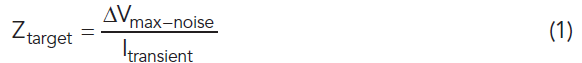
But, just using a target impedance alone as the design requirement is not enough. There are a few significant noise sources from the PDN elements that a simple target impedance does not adequately address. To be clear, the voltage regulation limits that must be maintained are made up of ripple noise from the VRM, DC regulation, IR drop, crosstalk from other power rails on die or on the board, and the voltage excursions due to dynamic transients. Target impedance only considers the voltage excursions due to dynamic current transients as the “noise source” that is being managed by the PDN impedance control.
The first correction to the target impedance design spec is to consider the other noise sources in the total budget and use the allocated fraction of the total noise budget in the dynamic transient current noise estimate. To keep the voltage-drop from the transient current below the acceptable voltage noise threshold, the impedance of the PDN, as illustrated in Figure 1, must be below a certain level: the target impedance.
When the Impedance Profile is Not Flat
If the impedance profile of the PDN, as seen by the IC pads, is a flat impedance profile from DC to the highest frequency components of the transient current, and we keep the flat PDN impedance below the target impedance, then the worst-case voltage noise, due to dynamic current, on the pads of the IC rail will be less than the maximum acceptable voltage noise.
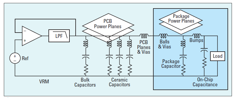
Figure 1. A simplified model of the PDN as seen by the pads of the die power rail
An important PDN design goal is to engineer a flat impedance profile for the PDN, below the target impedance. This is the basic criterion for a “robust” PDN. In this case, the worst-case voltage noise, due to dynamic current excitation, for a maximum transient current will always be less than the maximum acceptable noise.
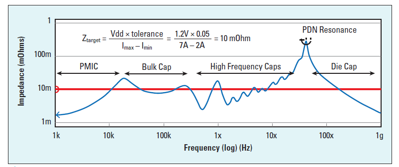
Figure 2. Impedance profile of the PDN as viewed from the pads on the die power rail
While a flat impedance profile is an important goal, in many cases, a flat impedance profile across the entire frequency range is too expensive to implement. There may be peaks in the impedance profile. These usually arise at the interfaces to the boundaries between the different interconnect elements, such as
- between the VRM and bulk decoupling capacitors
- between the bulk decoupling capacitors and the MLCC capacitors
- between the package lead inductance and the on-die capacitance
Figure 2 shows an example of a typical impedance profile of the PDN, as seen by the pads of the Vdd rail showing a few peaks, some larger than others. Using a target impedance as a design goal is a robust solution in the specific case of a flat impedance profile. When there are peaks in the impedance profile, the worst-case voltage noise is not accurately predicted by just a target impedance.
Engineering the peak impedances below the target impedance may make the PDN very expensive. This would require many MLCC capacitors, and thin dielectric between the power and ground planes, for example. Instead, a second criterion is introduced for acceptable performance where peaks occur.
The Features of an Impedance Peak in the PDN
Every impedance peak in the PDN is created by a parallel RLC circuit. Four terms characterize each peak:
- The parallel resonant frequency
- The characteristic impedance
- The peak impedance
- The q-factor
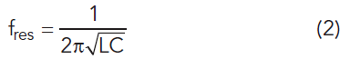
The parallel resonant frequency is the frequency at which the inductive reactance equals the capacitive reactance. This is calculated from
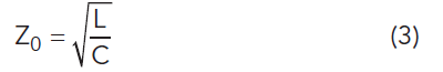
Used to characterize the RLC circuit, characteristic impedance is the impedance at which the reactive impedance of the capacitor equals the reactive impedance of the inductor, which occurs at the parallel resonant frequency. Do not confuse it with the characteristic impedance of a transmission line; it is just another impedance that characterizes the RLC circuit. The impedance where they cross, the characteristic impedance, is given by
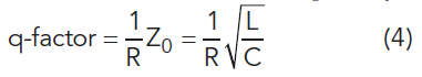
The q-factor of the peak is related to the damping created by any equivalent series resistance, the R term, from lead resistance, dielectric loss, or other interconnect resistance, and is given by
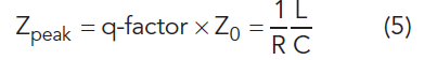
In the case of a q-factor greater than 1, the peak impedance is related to each of these terms by
The importance of these terms is seen when analyzing the voltage across the capacitor from two important current waveforms, a step response, and a square wave response.
Step Response of an Impedance Peak
As a first order model, the current draw from a die can be modeled as a current source. The bandwidth of a step current change, for a specific rise-time is given by
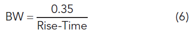
When the current source has a step current change with a rise-time shorter than 3.5 nsec, the bandwidth is greater than 100 MHz. If the parallel resonant frequency is below 100 MHz, then the voltage response of the RLC circuit to a step current change is a damped sine wave. The frequency of the damped sine wave is the parallel resonant frequency. The peak amplitude of the damped sine wave is given by
An example of this response is shown in Figure 3. This suggests when there is a step current change to keep the peak voltage noise on the PDN below the acceptable noise voltage, the characteristic impedance of each peak should be below the target impedance. If this is the case, then the worst-case voltage noise on the PDN will be less than the maximum acceptable level. This is the next most restrictive criterion for a robust PDN. Often, engineering the characteristic impedance to be below the target impedance is also an expensive choice.
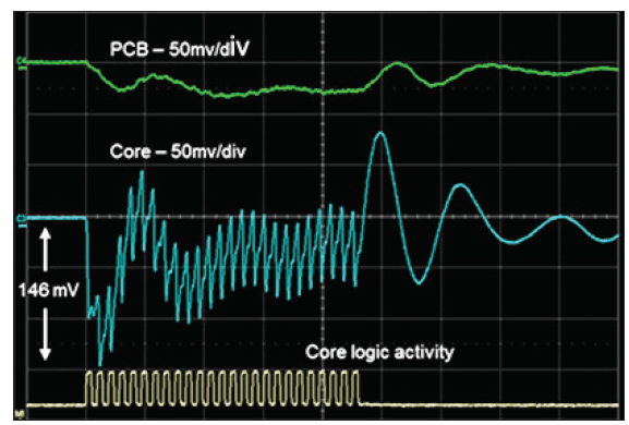
Figure 3. Measured on-die voltage noise of a power rail as the core logic current undergoes a step change in current load. Superimposed on the step current are the individual clock edge noise responses. Note the damped sine wave during the release
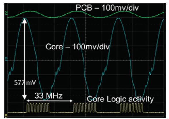
Figure 4. Measured voltage noise on a die when the core logic current is a square wave at the peak impedance frequency
Some risk might be acceptable that either there will never be a worse-case transient current with a short enough rise-time to excite the full peak, or this peak voltage noise might be acceptable if it is only present for a short period of time. But another current waveform may generate even more noise from a peak impedance in the PDN.
Resonant Response
When the transient current is in the shape of a square wave, with a repeat frequency exactly at the resonant peak frequency, the peak-to-peak voltage noise generated by the sine wave frequency component of the square wave of current at the parallel resonant frequency is
If the voltage on the die rail is at the nominal value, then this sine wave resonant response will be centered at the nominal value minus some IR drop. The noise excursion will be just the amplitude, which is half of this peak-to-peak value. The voltage above and below the nominal is:
The same transient peak-to-peak current, but at the resonant frequency, the resulting voltage noise excursion can be 0.64 × the q-factor × the step response voltage noise, both above and below nominal voltage. In some critical mission industries, the maximum voltage is important because the circuits are not allowed to be electrically overstressed. In other industries, the minimum voltage is important because of set-up time requirements, Vmin and Fmax considerations. It takes about a q-factor of cycles for the resonant square wave of current to drive the voltage noise to the peak voltage. A q-factor of 1/0.64 = 1.57 or more will result in a peak noise voltage exceeding the maximum allowable noise when the Z0 characteristic impedance meets the target impedance. But, to meet this criterion, not only must the maximum worst-case transient current modulate at the parallel resonant frequency, it must also be present for a q-factor of cycles to reach this worst case.
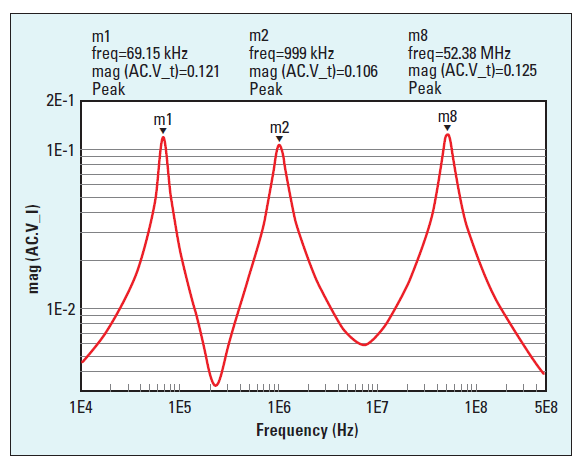
Figure 5. Impedance profile with three, high q-factor parallel resonant peaks. These occur at the boundaries of various PDN elements.
The larger the q-factor of the parallel resonance, i.e., the sharper the peak due to smaller damping, the larger the resonant response can be, but the longer the PDN must be driven to reach the full peak noise. Figure 4 is an example of the measured resonant response voltage on the die when a square wave of transient current drives the on-die PDN.
In a PDN designed to be fully robust and immune to resonant peak excitation, the worst-case voltage is below the acceptable noise threshold, so the parallel resonant peak impedance must be below 1.57× target impedance. The 1.57 factor comes because the positive and negative resonant excursions are 0.64 × Itransient × Zpeak, and the full voltage tolerance is reached at resonant conditions when an impedance peak is 1/0.64 = 1.57 × Ztarget.
The whole resonant waveform is biased and reduced by DC IR drop, so the voltage minimums may be farther away from nominal voltage than the voltage maximums. Reducing the impedance peak below this level will keep the worst-case peak-to-peak noise below the acceptable level when the resonance is fully stimulated. But this is often very expensive, especially when the resonant peak is from the on-die capacitance and package lead inductance.
Often, some risk is accepted based on the unlikely possibility of the worst-case transient current occurring exactly at the parallel resonant frequency and lasting for a q-factor of cycles. Many successfully deployed products have a peak height as large as 3× the target impedance. This is an impedance peak height 2× higher than a fully robust PDN.
But even a fully robust PDN, with all of its peaks below 1.56× the target impedance, may still have PDN voltage noise above the acceptable limit under a special set of conditions. This is when rogue waves may develop.
Rogue Waves
If the PDN impedance profile has two or more high q-factor parallel resonant peaks, each of which is below the target impedance, none of the peaks, if excited individually, might generate excessive voltage noise under worst case conditions.
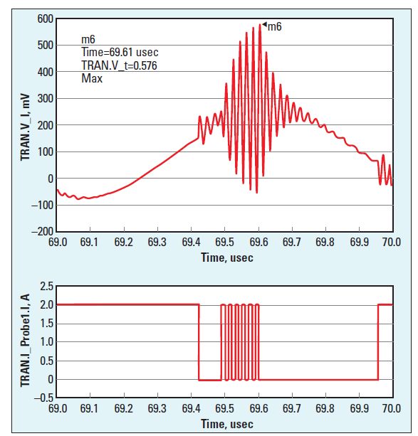
Figure 6. Rogue wave created by sequentially exciting two of the resonant peaks, by the current waveform shown in the lower graph
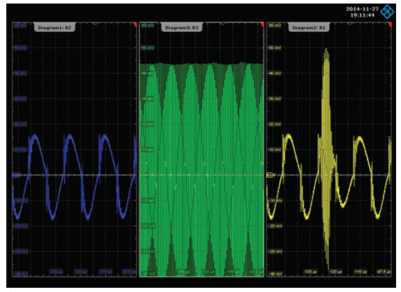
Figure 7. Measured voltage noise on a PDN from two different square waves of current with the same amplitude, exciting each resonance. In the far-right screen, these two excitations are phased exactly right to excite the rogue wave with a response larger than either of the two other responses
However, it is possible for a specific combination of resonant responses to sequentially build up exactly in phase to excite the lowest frequency peak, and then at its peak response, the second highest frequency peak, and at its peak, the highest frequency peak.
When multiple-frequency ocean waves add up exactly in phase, they can produce exceptionally large wave heights, which have been termed rogue waves. When multiple current waveforms are sequenced to excite multiple high q-factor peaks, the voltage noise on PDNs can show large peaks, which have been termed rogue waves.
Figure 5 is an example of the impedance profile of a PDN with three high q-factor parallel resonances. When this PDN is excited by at least two sequential groups of square waves of current, with a duration and phase exactly optimized, they can excite rogue waves on the PDN. Each square wave excites a different resonance, and the peak voltages build on each other. Even if each peak were below 1.56× the target impedance, meeting the fully robust requirement for acceptable noise, the resulting rogue wave of voltage can easily exceed the acceptable level of noise.
Figure 6 is an example of the simulated rogue wave on this PDN. How likely is it that the transient current waveforms from the core logic circuits would exactly match the specific resonant frequencies and stay on resonance long enough to excite the peak amplitude perfectly phased? In a critical application, it only must happen once, causing the voltage requirements to be exceeded. This can result in an overstress condition, or intermittent operation. Figure 7 is an example of the measured rogue wave response on a PDN from the unfortunate occurrence of exactly the right current waveform.
Conclusion
A robust PDN is engineered to have a flat impedance profile with an impedance below the target impedance. This should always be the design goal in every PDN. A flat impedance profile will eliminate the chance of resonant responses and provide a deterministic noise from the self-aggression Vdd currents. When the impedance profile is not flat, but has parallel resonant peaks, keeping the peak impedances below the target impedance is not enough of a criterion for a fully robust PDN.
Many designs are a balance between the performance, the risk, and the cost. When cost is an important driving force, an acceptable risk might be when a parallel resonance’s characteristic impedance is engineered to be below the target impedance. This would keep the peak voltage noise response from a step current to be within the acceptable noise limit.
But even this criterion is not robust enough for rare current waveforms. When resonant driving of peaks is possible, all impedance peak heights should be below 1.56× the target impedance. With multiple high q-factor peaks, even this condition is not enough for a fully robust PDN. Under rare conditions, a rogue wave with a voltage amplitude above the acceptable voltage noise limits may be created when multiple peaks are sequentially excited in phase.
Finally, a fully robust PDN would need to include the worst-case combination of all noise sources on each rail, from self-aggression noise and mutual-aggression noise. All designs are a tradeoff between the performance, the cost, the risk, and meeting the schedule targets. Each type of product has a different appropriate balance between these factors. In many consumer products, cost is the biggest driving factor and some risk is accepted. In high reliability products, low risk is the driving force and all of these effects must be included in any PDN analysis. The target impedance is a starting place to guide the design, but in low-risk products it is not enough of a criterion to base a design.
References
1. L. D. Smith and E. Bogatin, “Principles of Power Integrity for PDN Design—Simplified: Robust and Cost Effective Design for High-Speed Digital Prod-ucts,” Prentice Hall Modern Semiconductor Design, April 2017.
2. S. Sandler, “Power Integrity: Measuring, Optimizing, and Troubleshooting Power Related Parameters in Electronics Systems,” McGraw Hill Education, November 2014.
Article was published in the SIJ January 2019 Print Issue, Cover Feature: Page 8.