
Over the past many years I often received questions from my co-workers, friends and professionals in the industry to clarify the connection between the two seemingly independent and competing tasks and requirements of power distribution networks (PDN): delivering and supplying enough charge to the load in a timely fashion to avoid too much droop in the load voltage, versus achieving a required impedance target and the capability of capacitors delivering charge beyond their series resonance frequency. How are these requirements related to each other?
To correctly answer these questions, we first need to look at the broader picture and remind ourselves of a few fundamental facts and principles. Figure 1 shows a simplified one-dimensional block diagram of a point-of-load (POL) PDN, consisting of a DC source, bypass capacitors, PCB structure, package and silicon.
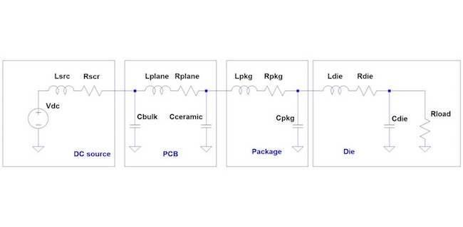
Figure 1: One-dimensional block diagram of end-to-end POL PDN.
In this block diagram there is a power source producing a nominally constant regulated DC voltage, low- and high-frequency bypass capacitors and the current consumer: the semiconductor device. All these are interconnected by conductors: PCB planes, power strips, puddles, vias and packages of the semiconductor (typically silicon) devices. Our goal is to provide sufficiently stable voltage to the load in spite of changes in its current draw.
Even though each block could also be represented by its multi-node distributed model, to get the answer to the opening questions, this simple lumped serial model is sufficient. As a fundamental requirement, we usually need the VAC AC transient voltage across the load to be much smaller than the nominal DC rail voltage Vnom DC load voltage that we want to maintain across the die. The typical ratio is one-and-half to two orders of magnitude: VAC is a few percent of Vnom. With the point-of-load scheme, we assume that noise at the silicon is primarily due to the fluctuations in current demand of the silicon: ‘crosstalk’ noise initiated by other loads in the system is neglected. Similarly, the noise generated by the power source is assumed to be either negligible or just a small portion of the worst-case noise on the supply rail. There are also series resistances along the path and the DC average current of the load will produce a DC drop between the DC source output and the load, or for cases where the DC source has a remote-sense connection, between the remote sense point (not shown here for sake of simplicity) and the load.
The DC source also has a finite tolerance and drift on its set output voltage. This is illustrated in Figure 2. The DC set-point accuracy and any uncompensated DC voltage drop is represented by the green bar on the voltage graph. The transient noise as a result of load-current fluctuations plus any DC-DC converter output ripple (in case the DC source is a switching regulator) are represented by the orange bar. Altogether, the DC voltage tolerance and DC drop together with the worst-case AC noise has to stay within the Vmax and Vmin voltage limits established for the silicon. For sake of simplicity here, we assumed no added margin, which can be easily added to this calculation if needed. Without restricting generality, symmetric voltage allocation was assumed, where the DC tolerance and AC tolerance bars are evenly placed above and below the nominal voltage. Dependent on the actual circuit details, in some of the real systems both the DC and AC tolerance bars may be arranged in an asymmetric way around the nominal voltage.
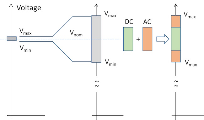
Figure 2: Voltage diagram of a supply rail illustrating the major design parameters.
While the AC voltage is expected to be a small fraction of the DC voltage, in many power rail designs we have to assume that the DC and AC currents of the load are comparable: if we do not have the AC transient current specified, a 50% value is assumed, namely the AC transient current is assumed to be half of the maximum DC current.
These time-domain requirements can be translated into the frequency domain. If we assume that on the rail we allow a ΔV worst-case voltage fluctuation as a result of ΔI current transients, we can call their ratio an impedance target [1].
Ztarget= ΔV ΔI
This impedance target calculation works well to predict the worst-case noise as long as we create a relatively flat and frequency independent PDN impedance at the load. With a flat (resistive) PDN impedance with Ztarget value, we guarantee that for any arbitrary sequence of DI current steps the resulting transient noise will not be bigger than ΔV [2]. Strictly speaking this also assumes that the entire PDN is linear and time invariant.
There are many instances when we can not, or for some reason do not want to, create a flat PDN impedance. As it was pointed out and explained in [3], [4] and [5], for non-flat impedances not exceeding the target impedance we pay a penalty of increased worst-case noise, where the penalty ratio depends on how much we distort the flat impedance. For typical non-flat impedance profiles that we find today in our designs, the penalty ratio does not exceed three, which gives a straightforward safe design process by designing for Ztarget/3.
We can also calculate the equivalent DC resistance of the load, which is the lowest at the maximum load current.
Rload=VDCImax
Whether we look at the voltages or impedances in a real situation, we will see that a good PDN is ‘stiff’: the voltage transients are small compared to the nominal DC voltage and likewise the PDN impedance presented to the load is much lower impedance than the load itself.
First we look at the middle of this chain: the bypass capacitors and conductors interconnecting the elements. The shunt elements in the PCB and Package blocks are discrete capacitors: Cbulk, Cceramic and Cpkg. These can cover a very wide range of types and constructions. The bulk capacitors can be electrolytic, tantalum, polymer tantalum or niobium capacitors in through-hole or surface-mount packages. The ceramic capacitors on the board and the package capacitors, which are typically also ceramic capacitors, are usually surface mount and may come in different case sizes and geometries: physically smaller and/or low-inductance (like reverse-geometry or interdigitated) package capacitors. On the boards, physically larger case sizes and higher capacitance values are used in regular two-terminal case styles. On a very fine scale, these capacitors all show some nonlinearities and time dependence [6]. However, given the fact that during normal operation the AC voltage across these capacitors is very small, the nonlinearities can safely be neglected. Similarly, even though capacitors do show time variance due to aging and time-dependent ambient temperature, for the duration of short transients, time dependence can be neglected. The same is even more true for the conductive interconnects: PCB planes, strips, patches, traces, vias and component pads can all be considered as linear and time invariant.
From all of the above, our first major conclusion is that in a well-behaved PDN, for the purposes of fast transient response calculations, the bypass capacitors and the PCB conductors can be modeled as linear and time-invariant elements.
Next, we make a few observations about the two ends of this chain, starting with the load. The semiconductor device is represented by its parallel Cdie capacitance, series Ldie inductance and Rdie resistance as well as Rload, representing the current consumption in digital devices due to leakage and power loss due to the voltage swings across device capacitances. In a logic device, like CPU or FPGA core, these elements represent the switching cells, these are naturally nonlinear elements. However, we earlier said that the PDN impedance should be much lower than the impedance of the load and therefore the load can be replaced by a current source representing the transient current. Though the nonlinearity is present in this case, due to the ratios of impedances, it does not matter.
Finally lets look at the DC source. It may be a battery, or a linear voltage regulator or a switching voltage regulator. Voltage regulators may be nonlinear, especially for large transient currents, but their bandwidth is limited; they can not respond to very fast current transients; exactly this is why we need bypass capacitors to supply the initial charge.
From these considerations, our second conclusion is that none of the end pieces of this PDN chain matter for fast transient calculations: the DC source does not have the bandwidth to respond to fast transients and the nonlinear silicon has much higher impedance than the PDN impedance and, therefore, –in first order- it can be modeled by (a linear) current source.
Now we can draw a generic conclusion and can give a generic answer to the opening question. For fast transient loads, the noise signature on the board will be highly independent from the DC source and the silicon load. The transient noise depends mainly on the bypass capacitors and PCB interconnects, which can be considered linear and time invariant. For linear and time invariant networks, the time and frequency domain descriptions are equivalent, and, therefore, we can look at the results in whatever domain we are more comfortable with or whatever domain provides the necessary information more easily or in an easier-to-understand form. If the requirements are correctly set, it does not matter whether they are set in the frequency or in the time domain, for linear and time invariant systems they yield the same results.
In the rest of the article we look at typical numbers and waveforms to illustrate these conclusions.
In Figure 3 we added typical numbers to represent the PDN for a hypothetical 10W FPGA core running at 1GHz. Starting on the right, the 0.1-Ohm Rload value simply comes from the 10W dissipation and 1V supply-rail voltage. The Cdie capacitance can be estimated from the clock frequency and power dissipation. If we neglect the leakage current, each edge of the clock signal creates a dissipation of
E=12CV2
Since each clock period has two edges, the total dissipated power becomes
P=CV2ƒ
If we rearrange the above equation, we get Cdie = 10 nF.
The 10 pH inductance and 0.1 mOhm resistance represent the resistance and inductance of the power grid on the silicon.
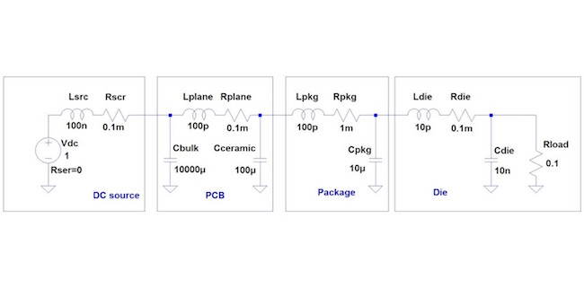
Figure 3: One-dimensional block diagram of end-to-end POL PDN with typical numbers for a 1V/10W/1GHz core rail.
The bulk capacitors, ceramic capacitors and package capacitors are represented single capacitors, but in many designs we have multiple pieces in each category; the values in Figure 3 represent the cumulative result of multiple pieces. Figure 4 shows the impedances of the four capacitor banks as stand-alone capacitors, without their interactions. Note that the actual values may strongly depend on the nature of the design. We can calculate the series resonance frequencies of each capacitor bank from their capacitance and inductance values. Table 1 shows the calculated Series Resonance Frequency (SRF) values calculated from the parameters used in the SPICE simulations.
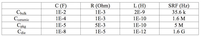
Table 1: C-R-L equivalent values and the calculated SRF for each capacitor bank.
We can follow these values in Figure 4 and can identify the frequency ranges, where according to popular belief, these capacitors can efficiently supply charge. For instance, the ceramic capacitor bank’s 1.6 MHz SRF suggests that these capacitors may not be able to supply charge much faster than one microsecond.
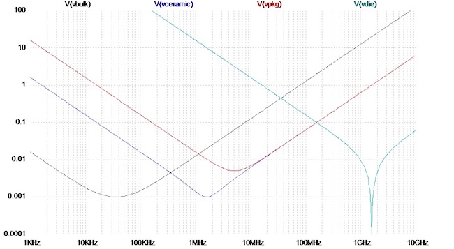
Figure 4: Impedance of the four capacitors banks in Figure 3’s circuit. The horizontal axis is frequency, vertical axis shows impedance magnitude in Ohms.
Before we look at the time-domain results, we should also look at the impedance plot cumulatively from the entire PDN. Figure 5 shows the impedance magnitude simulated across Cdie. We see three resonance peaks; these correspond to the inter-resonances between the capacitor banks. For instance, the 200 MHz peak with 0.1-Ohm peak value is the die-package resonance, created by the package inductance and die capacitance.
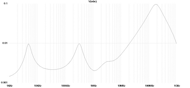
Figure 5: Impedance magnitude of the PDN shown in Figure 3, as seen across Cdie.
If we take a very fast current edge, representing a sudden current demand from the silicon, the simulated transient currents supplied by the four capacitor banks are shown in Figure 6. Note that in order to show the several orders of magnitude frequency range across which these capacitors operate, the horizontal time scale is logarithmic. The blue trace is the excitation current: we assume that 50% of the maximum sustained current is the step magnitude with a 200 ps rise time.
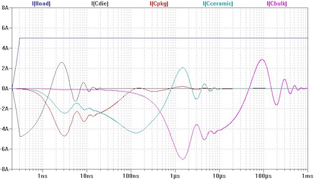
Figure 6: Transient current in the PDN capacitors in response to a 5A 200 ps current step.
The black trace shows the current in the die capacitance. It carries all the initial transients up to about 10 ns time, after which its current diminishes. We can notice that in the few hundred picoseconds time window only the die capacitance supplies the current: the series inductances prevent the other capacitors from taking part. About half a nanosecond after the initial current step, the package and board ceramic capacitors start to supply current. The package capacitor’s current dies out after 100 ns, the board ceramic capacitors keep supplying current for up to about 3 microseconds. Finally the bulk capacitors step in around 100 nanoseconds and supply current for about one millisecond. After a millisecond, the DC power supply carries the current.
Conclusion
The impedance plot of Figure 5 shows that when we consider the entire chain of power distribution components, antiresonances can build up along the way, and the current waveforms of Figure 6 tell us that capacitors can also supply transient currents way above their series resonance frequencies. As we concluded earlier, as long as we model the PDN with linear elements, the time- and frequency-domain descriptions carry equivalent information.
References:
[1] Larry D. Smith, Raymond E. Anderson, Douglas W. Forehand, Thomas J. Pelc, and Tanmoy Roy, ‘‘Power distribution system design methodology and capacitor selection for modern CMOS technology’’, IEEE Transactions on Advanced Packaging, vol. 22, no. 3, pp. 284-291, Aug.1999.
[2] Drabkin, et al, “Aperiodic Resonant Excitation of Microprocessor power Distribution Systems and the Reverse Pulse Technique,” Proceedings of EPEP 2002, p. 175.
[3] “Bypass Capacitor Selection Based on Time Domain and Frequency Domain Performances,” in TecForum TF-MP3 "Comparison of Power Distribution Network Methods"
[4] “Systematic Estimation of Worst-Case PDN Noise: Target Impedance and Rogue Waves,” QuietPower column, 2015, available at
[5] “How to Design a PDN for Worst Case?” QuietPower column, 2015
[6] “Dynamic Models for Passive Components,” QuietPower column, 2016