Simulation Results
A simulation model of the inner and outer equalization study is presented in Figure 13,
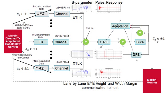
Figure 13: Inner and outer EYE equalization simulation model
Simulation is conducted with long channel, medium, and short channels using a typical active CTLE. The receiver is optimized stand-alone at the pre-back-channel operation phase. Then, during the back-channel operation phase, transmitter figure of merit (FOM) optimization is performed by doing a grid search of the pre-cursors and post cursors.
Long-channel simulations were done with transmitter launch set to 1300mV and 800mV. The vertical margin and horizontal margin contour plots are plotted in Figure 14 and Figure 15. It is evident that 800mV launch has significantly relative low voltage margin compared to 1300mV, indicating higher transmitter launch voltage is desirable for long channel. After certain TX launch, amplitude compression starts to kick in due to reduced signal headroom in limited power supply analog front end.
Short-channel simulation is done with transmitter launch set to 1300mV and 800mV. The vertical margin and horizontal margin contour plot shown in Figure 16 and Figure 17. They show that even after reducing the transmitter amplitude to 800mV the operating margin is far better than long-channel operating EYE margin.
Having EYE height margin beyond certain threshold does not buy any jitter tolerance performance. In order to reduce the operating system power the transmitter launch amplitude can be reduced for a short channel. This in turn reduces the system XTLK floor due to reduced transmitter launch amplitude in short channel, benefiting stressed long channel operating margin.
Thus, the application of an outer-equalization loop has the potential to offer improved long-channel performance and to reduce overall system operating power by lowering the transmitter amplitude in shorter reach lanes.
Long Channel Simulations
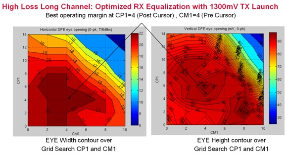
Figure 14: Long channel horizontal (%UI) and voltage (peak mV) margin as a function of CP1/CM1 for optimized receiver settings with high TX amplitude
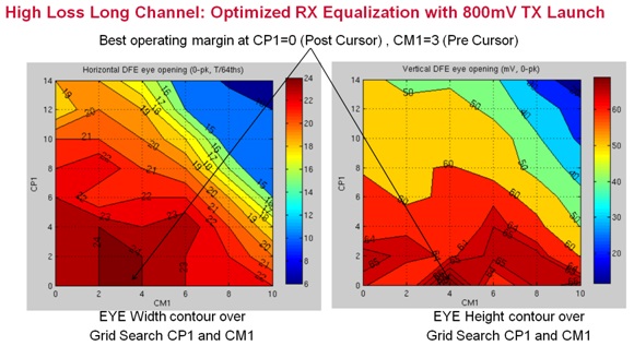
Figure 15: Long channel horizontal (%UI) and voltage (peak mV) margin as a function of CP1/CM1 for optimized receiver settings with low TX amplitude Short Channel Simulation
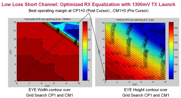
Figure 16: Short channel horizontal (%UI) and voltage (peak mV) margin as a function receiver CP1/CM1 for fixed optimized receiver settings with high TX amplitude

Figure 17: Short channel horizontal (%UI) and voltage (peak mV) margin as a function receiver CP1/CM1 for fixed optimized receiver settings with low TX amplitude
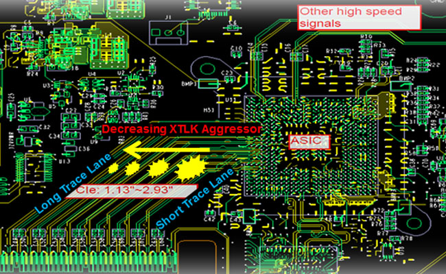
A crosstalk sensitivity study is performed to evaluate the impact of transmitter amplitude, transmitter slew rate, and transmitter pre and post cursor on EYE height and width margin at a victim receiver. In this study, one NEXT channel closes to the victim receiver and one FEXT channel closest to the victim receiver is used as shown in Figure 18.
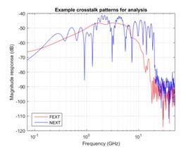
Figure 18: Worst- case NEXT and FEXT frequency response used in the simulation
Simulations were done with the PCIe reference receiver to quantify the XTLK impact at a victim receiver due to transmitter amplitude, slew rate, and de-emphasis at the aggressors. This study helps us in identifying the priority for adjusting the transmitter amplitude, slew rate, and pre/post emphasis in XTLK mitigation scheme using outer equalization layer exploiting the Lane Margin feature of the PCIe Gen4 transceivers. The results of the study are presented next.
XTLK Path Transmitter Amplitude Sensitivity Study
The XTLK impact due to transmitter launch amplitude is determined by exciting the selected NEXT and FEXT with varying transmitter amplitude with near perfect rise time signal (sharp rise time is used to excite XTLK spectrum beyond Nyquist frequency). The contour plot of the calculated RMS XTLK in mV is presented in Figure 19.
The contour plot shows that with increasing transmitter amplitude at the aggressor transmitter, the RMS XTLK is increasing at the victim receiver data decision latch input. It also shows that the NEXT XTLK impact is slightly higher than the FEXT XTLK as one would expect. In this S-parameter example, a NEXT aggressor transmitter launching at 825mV creates 2.1mV RMS XTLK at victim receiver, while a FEXT aggressor transmitter launching at 1060mV creates 2.1mV RMS XTLK at victim receiver.
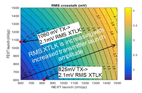
Figure 19: XTLK path transmitter amplitude impact on victim receiver
XTLK Path Slew Rate Sensitivity Study
The XTLK impact due to transmitter rise/fall time is determined by exciting the selected NEXT and FEXT S-parameter by sweeping the 20%-80% rise fall time and by setting the transmitter amplitude to 1000mV, pre and post emphasis to 0dB. The contour plot of the calculated RMS XTLK in mV is presented in Figure 20. Sharp rise/fall time creates high-frequency spectral contents in the transmitted signal beyond Nyquist frequency. The contour plot clearly demonstrates increasing RMS XTLK with decreasing rise/fall time.
In the case of FEXT, the high-frequency spectral contents will be attenuated as a function of channel length induced insertion loss. However, in the case of NEXT from neighboring aggressors, the high-frequency spectral energy does not get attenuated due to the close proximity of the aggressor channels.
The contour plots shows that 0.15UI rise/fall time from NEXT injects 2.7mV RMS XTLK in to the victim receiver, while for FEXT 0.45UI rise time injects the same amount of RMS XTLK in to the victim receiver. As a result, the NEXT path rise/fall time equalization through outer equalization has higher priority than the FEXT path rise/fall equalization.
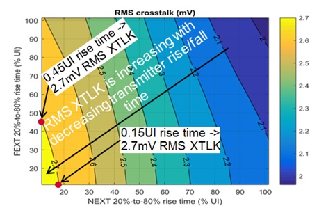
Figure 20: XTLK path transmitter slew rate impact on victim receiver
XTLK Path Transmitter Pre/Post De-Emphasis Sensitivity Study
The XTLK impact of the aggressor channel transmitter de-emphasis due to pre-cursor or post-cursor equalization is presented in Figure 21. In general, due to the application of transmitter de-emphasis, the average signal amplitude out of the transmitter is reduced and that helps to contain the system XTLK floor, as long as the rise/fall time of the Nyquist signal is not very aggressive. For all practical purposes, one would reduce the rise/fall time to have effective equalization coming out if the transmitter, but care must be given not to be too aggressive with rise/fall time in a system where XTLK sensitivity is an issue due to isolation issues in a package, at the connectors, or on the PCB board itself.
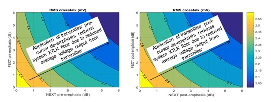
Figure 21: XTLK path transmitter pre/post emphasis impact on victim receiver
Now we demonstrate the impact of the RMS mV XTLK on equalized signal EYE height (noise margin) and width (jitter margin) using the PCIe Gen4 reference CTLE. In this study, we use XTLK generated using RMS mV FEXT and NEXT using 1000mV, 0.32UI slew rate, and 0dB pre and 0dB post emphasis. We scale the NEXT and FEXT XTLK between 0 to 5mV and determine EYE margin using the PCIe reference CTLE and tap limited PCIe 2-tap DFE. We also sweep reference CTLE peak frequency between 3GHz to 10GHz to demonstrate the effect of out of band NEXT/FEXT on EYE margin. In a practical receiver, CTLE peaking frequency will vary over process-voltage-temperature (PVT) corner.
In Figure 22 and Figure 23, we present simulations results with 800mV and 1300mV to evaluate the impact of RMS XTLK floor on EYE margin. We also show the impact of CTLE peaking frequency positioning on EYE margin. In the left-hand-side plots, we show that as the RMS XTLK increases, the EYE height is decreasing. We also show that as the peaking frequency is increasing, the EYE height is also decreasing by not suppressing the high frequency XTLK in this passive CTLE. Plotting differently, the right-hand plots show that optimal CTLE peaking frequency is at around 3GHz-5GHz. As the CTLE peaking frequency is increasing, the EYE height is decreasing, allowing more XTLK to come in band with the signal as indicated in Figure 22.
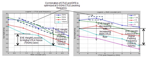
Figure 22: Effect of RMS XTLK and CTLE peaking frequency on EYE height at 800mV transmitter amplitude
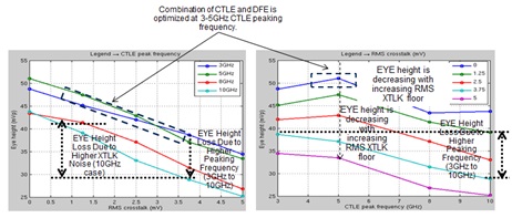
Figure 23: Effect of RMS XTLK and CTLE peaking frequency on EYE height at 1300mV transmitter amplitude
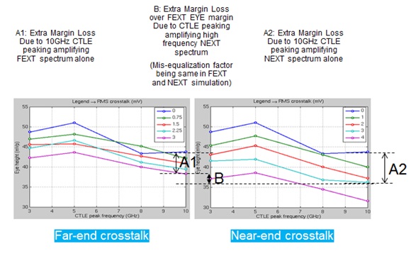
Figure 24: NEXT has higher frequency content and has larger performance degradation compared to FEXT
In Figure 24, the impact of NEXT and FEXT terms are separated to test performance sensitivity to these individual crosstalk components. NEXT has relative greater amount of high-frequency content compared to FEXT as shown in Figure 18. In Figure 24, A1 (A2) denotes eye height degradation due to FEXT (NEXT) of 3mV RMS level with CTLE peak frequency of 10GHz, and B denotes the extra loss with NEXT vs. FEXT.
As CTLE peak frequency increases beyond the optimal setting, the signal mis-equalization component increases equally for both the FEXT and NEXT cases, whereas the crosstalk-related component increases faster with NEXT. As a result, it would be better to reduce NEXT component seen by the weakest link in the system by adjusting launch amplitude or rise/fall time in the neighboring crosstalk contributors. Performance can also be improved by better optimizing CTLE peak frequency in the victim path receiver.
In this study, we presented a quantitative evaluation of the impact of the transmitter amplitude, slew rate, and pre/post emphasis on the RMS XTLK floor in a system consisting of a plurality of PCIe lanes. Through simulation, we demonstrated the impact of the RMS XTLK floors vs. EYE margin at the victim receiver. We also showed the impact of the CTLE peaking frequency in victim receiver EYE margin in presence of XTLK. The outer equalization layer optimizes the overall system performance through controlling the transmitter signal amplitude, slew rate, and pre and post de-emphasis such that lanes with excess margin can operate at reduced transmitter amplitude and increased rise/fall time for reducing system XTLK noise floor. It also allows increasing transmitter amplitude and slew rate for the most stressed lanes if needed.
Conclusion
PCIe Gen4 introduces lane margining as a required feature that gives a downstream port access to the SerDes internal operating EYE margin. The implications of this feature are far reaching and are expected to enable system-level equalization schemes for managing XTLK, system operating margin tuning for high-volume manufacturing, and field diagnosis and tuning of marginal systems through outer-layer equalization, on site or remotely. A new wave of innovation is enabled to guide inner-loop SerDes optimization assisted by outer loop system optimization. In this study, we explored the protocol aspect, algorithm aspect, and performance aspect of the outer loop equalization using the Lane Margin scheme.
The data in this paper was originally presented at DesignCon 2017 and was a Best Paper Award winner.
Download the full paper here
References
[1] PCIe Gen4 standards draft 0.7 May, 2016, in approval state by the working group
[2] SAS4 standard sas4r06, Working draft American National Standard, Project T10/BSR INCITS 534, revision 06, 11 May 2016
[3] IEEE Standard for Ethernet, IEEE Computer Society, IEEE Std 803.3TM, 2015
[4] PCIe Base: Margining capabilities, 19 May, 2016. Working Draft, Revision 4.0, 0.7 Maturity Level.
[5] RX Margining Extended Capability, 14 January, 2016, Working Draft, Base 4.0 – 0.65 Maturity Level.
[6] Alternate RX Margin Proposal, Gerry Tablot, Dan Froelich, Debendra Das Sharma, PCI-SIG, October 13, 2015.
[7] RX Margining during L0 in PCIe 4.0, PCI-SIG, February, 24, 2016.
[8] PHY Interface for the PCI Express, SATA, and USB 3.1 Architectures, version 4.3 (With ongoing definition for PCIe Gen4 Margin Interface, unpublished as of November, 2016)
[9] Mohammad Mobin, et al, “SerDes Steady State Adaptation Challenges in Existing SAS/SATA and Emerging PCIe Gen4/SAS4 Application and their Solutions with Pattern Discriminator Constrained Adaptation”, DesignCon 2015.
[10] Mohammad Mobin, et al, “On the validity of lumped jitter approximation in the statistical analysis of SerDes”, DesignCon 2013.
[11] Mohammad Mobin, et al, “Comparative Evaluation of 16 GT/s PCIe Gen-4 and 22.5 GT/s SAS-4 Standards Evolution and their Impact on Future Systems and SerDes”, DesignCon 2016.
[12] Mohammad Mobin, et al, “TX back channel adaptation algorithm and protocol emulation with application to PCIe, SAS, FC, and 10GBASE-KR”, DesignCon 2012
[13] Deutsch, Alina. "Electrical characteristics of interconnections for high-performance systems." Proceedings of the IEEE 86.2 (1998): 315-357. http://ieeexplore.ieee.org/stamp/stamp.jsp?arnumber=659489
[14] Buckwalter, James F., and Ali Hajimiri. "Cancellation of crosstalk-induced jitter." IEEE journal of solid-state circuits 41.3 (2006): 621-632. http://ieeexplore.ieee.org/stamp/stamp.jsp?arnumber=1599531
[15] Pelard, Cattalen, et al. "Realization of multigigabit channel equalization and crosstalk cancellation integrated circuits." IEEE journal of solid-state circuits39.10 (2004): 1659-1670. http://www.bioee.ee.columbia.edu/courses/upload/Bibliography/pelard_jssc_2004.pdf
[16] Sham, Kin-Joe, et al. "FEXT crosstalk cancellation for high-speed serial link design." IEEE Custom Integrated Circuits Conference 2006. IEEE, 2006.
[17] Nazari, Meisam Honarvar, and Azita Emami-Neyestanak. "A 15-Gb/s 0.5-mW/Gbps two-tap DFE receiver with far-end crosstalk cancellation." IEEE Journal of Solid-State Circuits 47.10 (2012): 2420-2432. http://ieeexplore.ieee.org/stamp/stamp.jsp?arnumber=6248710
[18] Lu, Jian-Hao, and Shen-Iuan Liu. "A merged CMOS digital near-end crosstalk canceller and analog equalizer for multi-lane serial-link receivers."IEEE Journal of Solid-State Circuits 45.2 (2010): 433-446. http://ieeexplore.ieee.org/stamp/stamp.jsp?arnumber=5405140
[19] Jung, Hae-Kang, et al. "A 4 Gb/s 3-bit parallel transmitter with the crosstalk-induced jitter compensation using TX data timing control." IEEE Journal of Solid-State Circuits 44.11 (2009): 2891-2900. http://ieeexplore.ieee.org/stamp/stamp.jsp?arnumber=5308594
[20] Lee, Seon-Kyoo, et al. "A 5 Gb/s single-ended parallel receiver with adaptive crosstalk-induced jitter cancellation." IEEE Journal of Solid-State Circuits48.9 (2013): 2118-2127. http://ieeexplore.ieee.org/stamp/stamp.jsp?arnumber=6548094
[21] Oh, Taehyoun, and Ramesh Harjani. "A 6-Gb/s MIMO crosstalk cancellation scheme for high-speed I/Os." IEEE Journal of Solid-State Circuits 46.8 (2011): 1843-1856. http://ieeexplore.ieee.org/stamp/stamp.jsp?arnumber=5871283
[22] Oh, Taehyoun, and Ramesh Harjani. "A 12-Gb/s multichannel I/O using MIMO crosstalk cancellation and signal reutilization in 65-nm CMOS." IEEE Journal of Solid-State Circuits 48.6 (2013): 1383-1397. http://ieeexplore.ieee.org/stamp/stamp.jsp?arnumber=6492120
[23] Hur, Youngsik, et al. "Equalization and near-end crosstalk (NEXT) noise cancellation for 20-Gb/s 4-PAM backplane serial I/O interconnections." IEEE transactions on microwave theory and techniques 53.1 (2005): 246-255. http://ieeexplore.ieee.org/stamp/stamp.jsp?arnumber=1381695
[24] San K. Chhay , et al. “Crosstalk Mitigation in Dense Microstrip Wiring Using Stubby Lines” Intel Corporation, http://ieeexplore.ieee.org/stamp/stamp.jsp?tp=&arnumber=6703506
[25] Jimmy Hsu, et al. “Broad-side Crosstalk Mitigation in Dual-Stripline Designs” Intel Corporation, http://ieeexplore.ieee.org/stamp/stamp.jsp?tp=&arnumber=6249107
Author(s) Biography
Mohammad S. Mobin earned his PhD in electrical engineering from Southern Methodist University. He also holds MSEE and BSEE from University of South Alabama and Bangladesh University of Engineering and Technology. For last ten+ years M. S. Mobin is involved with SerDes architecture definition, system modeling and simulation. He is deeply involved with channel equalization and timing recovery techniques. Currently he is a distinguished engineer at Broadcom Ltd. He has 100 US patents granted in his name; he published various papers in IEEE transactions in Biomedical Engineering, and other conferences. He represents Broadcom Ltd in PCIe EWG Standards Committee.
Haitao (Tony) Xia is Director of R&D at Broadcom Ltd, leading the research and development of advanced read channel and Serdes architectures for data storage systems. Dr. Xia served as Chairman of IEEE Data Storage Technical Committee and President of Chinese American Information Storage Society (CAISS) in the past. Before his work at Avago/LSI, Dr. Xia worked at Silicon Valley start-up, Linked-A-Media Devices, on signal processing and coding in the area of magnetic recording channels and non-volatile memories. Dr. Xia has published more than 20 articles in peer-reviewed journals/conferences, and has more than 100 US patent granted to his name. Dr. Xia is an IEEE Senior Member.
Aravind Nayak is a principal engineer with Broadcom Ltd in Allentown, PA. He holds PhD (2004) and MS (2000) degrees in electrical engineering from the Georgia Institute of Technology, Atlanta, GA, and B. Tech (1999) degree in electrical engineering from the Indian Institute of Technology, Madras, India. His research interest include signal processing for the magnetic recording read channel and SerDes applications.
Gene Saghi is a principal engineer with Broadcom Ltd. He earned a PhD from Purdue University, a MEng degree from Cornell University, and a BS degree from Wichita State University; all in electrical engineering. He has over 30 years of engineering experience ranging from board-level design to ASIC design to teaching and research in electrical engineering at the university level. Currently, he is a hardware architect working on IO controllers and RAID-on-Chip controllers. He represents Broadcom Ltd on the PCI Express Protocol Working Group committee.
Christopher J. Abel is a Director of Engineering at Broadcom Ltd, responsible for analog and mixed-signal design for SerDes IP in the Data Controller Division. He has focused on analog and mixed-signal IC design for more than 20 years, and on SerDes design for the last 15 years. He holds more than 20 US patents in the areas of analog design, data converters, and SerDes. Chris received the Ph.D. degree in electrical engineering from The Ohio State University, Columbus, OH, USA, in 1995.
Lane A. Smith is a Director of Engineering at Broadcom Ltd, responsible for storage SerDes design and SAS/SATA Protocol design. He has over 25 years of engineering experience ranging from design to management of several generations of modem and Fibre Channel, SAS, SATA, PCIE SerDes designs. He has over 100 US patents granted in his name in the area of modem, audio codec and SerDes design.
Jun Yao is currently a senior architect engineer with Broadcom Ltd in San Jose. Before joining Avago, he worked as a postdoctoral researcher at Carnegie Mellon University, PA. He obtained his PhD degree (2013) in electrical and electronic engineering from Nanyang Technological University, Singapore, and bachelor degree (2008) from Harbin Institute of Technology, China. His research interests include signal processing, equalization, phase-locked loop, detection and decoding algorithms for the hard disk drive (HDD) read channel and high-speed Serializer/Deserializer (SerDes) communications.