
The design and performance of power distribution networks (PDNs) in modern printed circuit board (PCB) assemblies and application-specific integrated circuits (ASICs) are paramount for ensuring a stable and clean voltage to the load.1 To achieve this, accurate modeling of all elements of the PDN is essential.2 One often overlooked element is an accurate representation of the capacitors that filter voltage ripple at the load and provide a matched impedance from the source to the load. Capacitors are an integral part of any PDN, yet the models used can be compromised by additional inductance introduced during the measurement process. This added inductance creates an error term in the model that affects the capacitor’s impedance’s accuracy and impacts the PDN’s quality.
This error term comes from failing to properly de-embed the measurement mount when characterizing capacitors. Many vendor-provided capacitor models contain extra inductance from the measurement mount that can result in inaccuracies in the representation of capacitor parameters, such as the resonance frequency, equivalent series resistance (ESR), and equivalent series inductance (ESL).1 This error term can then lead to errors in the simulation of the PDN, concealing resonant Q-points or causing unnecessary over-design efforts to mitigate inductance that does not exist in the physical PDN.
This further emphasizes the importance of proper calibration, measurement, and de-embedding to ensure that the final capacitor model is free of errors, allowing an accurate representation of the PDN used in simulation.3 While capacitor models may play a seemingly minor role in the overall system design, the impact of capacitor models can significantly impact the system design and, importantly, design sign-off.
How to Measure Passive Components
Correct and error-free measurements result from proper equipment, calibration techniques, and correlation to known good measurements.4 Figure 1 shows an image of a frequency response analyzer (FRA), used as a vector network analyzer (VNA), measuring a device under test (DUT). In this case, the DUT is a 0402-capacitor mount board that has been purposely shorted. The measurement of this shorted 0402 mount is then used later to de-embed the mount from measurements of capacitors with 0402 package size. Due to the variety of capacitor sizes, package-specific mount boards are required to hold the capacitors for measurement.
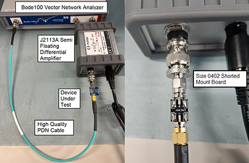
Figure 1. Image of a shorted mount measurement.
A variety of VNAs, cables, and mounts can be used if they are correctly calibrated and measured. All sources of error in the cables and DUT must be addressed as part of the calibration process. In a 2-port impedance measurement setup, it has been well documented that a ground loop is present and adds error to the measurement result.5 In Figure 1, the J2113A semi-floating differential amplifier is used in the measurement setup to break the inherent ground loop in the measurement path.6
Measurement to Simulation Correlation of a Shorted Mount
An electromagnetic (EM) model of the mount is extracted from the PCB artwork using the finite element method field solver in Keysight PathWave PIPro to build confidence in the measurement. This EM extraction is a Touchstone file in the S-parameter format. Resistive and ground losses are included in the EM model extraction. The EM extraction setup consists of an ideal 0 Ω resistor across the capacitor pads to represent a perfect short. A 3D representation of the model is shown in Figure 2.
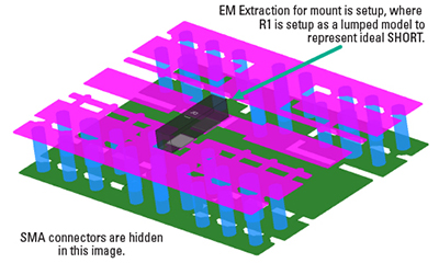
Figure 2. EM model of short board.
Figure 3 shows the results of the extraction. The shorted 0402 mount board has a low-frequency resistance of 0.49 mΩ up to 10 kHz, as seen with marker m2. At frequencies higher than this, the impact of the mount board’s inductance takes over. Marker m3 is placed at 10 MHz, and the measured impedance is 0.036 Ω. Equation (1) gives the inductance of the mount for a given reactance XL at a frequency f. The shorted 0402 mount inductance is 580 pH.
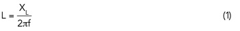
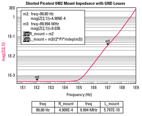
Figure 3. EM extraction results of shorted 0402 board.
Figure 4 shows the results comparing the measurement with the EM extraction of the 0402 shorted mount. There is a strong correlation between the EM extraction and the measurement of the shorted mount. The EM extracted PCB mount’s path inductance is 580 pH, while the measured PCB mount’s path inductance is 520 pH. This difference of just 60 pH gives confidence that the simulated model is an accurate way to de-embed the mount.
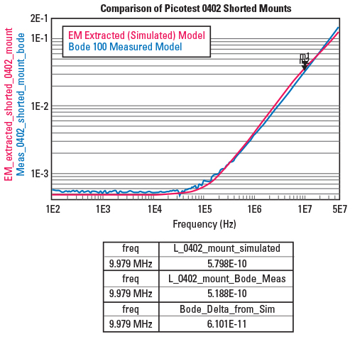
Figure 4. Comparison of Picotest 0402 shorted mounts, extraction to measurement.
Why Do We Care So Much About the PCB Mount?
The capacitor mount adds error to the capacitor measurement. The extent of this error varies by the mount used due to dependencies on the arrangement of vias, dielectric material, and copper trace thicknesses. These dependencies warrant that the best method of de-embedding the fixture from a mounted DUT measurement utilizes a characterization of the isolated mount itself. Figure 5 illustrates that the measurement reference points move from the SMA connectors to the capacitor terminals by de-embedding the mount board from the mounted DUT measurement.
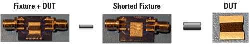
Figure 5. Graphic of DUT and mount board.4
How Does De-embedding Work?
De-embedding takes the overall mounted DUT measurement S-parameters and removes the known parameters of the measurement mount board. In Figure 4, the measurement mount is shorted together with bus wire and measured, and is then compared to the EM extraction of the same measurement mount shorted. The correlation between these two provides confidence that the parameters of the mount board are known and can be removed from the overall measurement S-parameters. What remains are just the S-parameters of the capacitor.8
Why does this matter? A power distribution network is robust if its capacitors help provide a matched impedance from source to load. The impedance versus frequency response of the capacitor is a function of the capacitance, its ESL, and ESR. If the PDN simulation uses capacitors with uncorrected error terms in the ESL, the results of the entire simulation are affected.
Currently, passive component models from vendors do not follow a set measurement and de-embed standard. Figure 6 compares a de-embedded and not de-embedded measurement of a 0.1 μF 0402 capacitor against models provided by vendors. Both vendor capacitors had the same voltage and dielectric material. However, notice how the resonance peaks and valleys in the simulation will not line up with measurement due to additional error terms attributed by each capacitor.
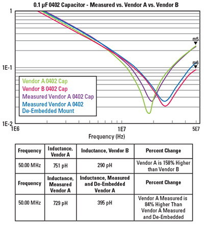
Figure 6. Comparison of a 0.1 μF 0402 vendor models to measurements.
The model from Vendor A has an inductance of 751 pH at 50 MHz, shown as the green line, while the model from Vendor B only has an inductance of 290 pH, shown as the red line. Looking further, the Vendor A 0402-capacitor measurement with the mount board included has an inductance of 729 pH, shown as the purple line, which is very similar to the Vendor A model. When that same capacitor is measured and then de-embedded, the capacitor inductance is only 395 pH, shown as the blue line, and is about what is expected.3 This demonstrates that the Vendor A capacitor likely was not properly de-embedded and has an additional 400 pH of inductance in the model. Vendor A’s model has 158% more inductance than Vendor B’s model. Vendor A’s model also has 84% more inductance than Vendor A’s capacitor measured and de-embedded. This lack of de-embedding the measurement mount has been seen on models across many vendors. On a PDN with many capacitors, this error term quickly adds up, causing a significant impact on the accuracy of the simulation.
Complete PDN Simulation with Vendor Capacitor Models and Measurement-Based Capacitor Models
To fully emphasize the impact of the additional ESL in vendor capacitor models, a complete system PDN design was simulated with both vendor and measurement-based capacitor models. This PDN design uses a 0.8 V voltage power domain to supply current to the core rail, DDR, and PLL circuitry on a custom ASIC, Project Alpha. The complete system PDN model is illustrated in Figure 7 and shown as a block diagram in Figure 8.
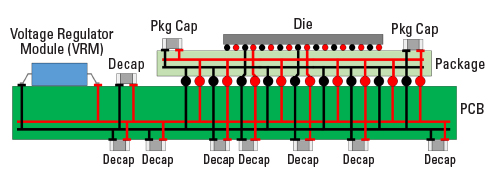
Figure 7. Project Alpha VDD_DDR_CORE full system PDN layout.
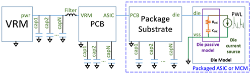
Figure 8. Project Alpha VDD_DDR_CORE full system PDN simulation block diagram.
The Keysight Advanced Design System (ADS) simulation schematic is shown in Figure 9. This consists of a Sandler State-Space Average Model (SSAM)10 of the LTM4650-2 Voltage Regulator Module (VRM); the PCB PDN; the substrate PDN (including a remote sense point on the substrate); a power manager LTC2977; and die models for the core rail, DDR, and PLL circuitry.
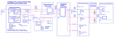
Figure 9. Project Alpha full system PDN simulation model with VDD_CORE and VDD_DDR die models.
The PCB and substrate models are EM extractions of the artwork and include ports for attaching the decoupling capacitor models, as shown in the sub-PDN models of Figures 10 and 11.
Figure 10. Sub-PDN model containing extracted PCB artwork with vendor capacitor models.
Figure 11. Sub-PDN model containing extracted substrate artwork with vendor capacitor models.
The capacitor models are either vendor models or lumped element broadband SPICE models fitted to the de-embedded S-parameter measurements of the actual capacitors to ensure simulation coverage outside the frequencies in the measured S-parameter model. These core and DDR die models contain piece-wise linear waveforms representing time domain current demands on the PDN. The passive and active current die models are SPICE extractions from the die circuitry designs, extracted using Cadence Voltus. This system model allows both frequency domain and time domain analysis.
The simulation results of Figure 9 (using the sub-PDNs shown in Figures 10 and 11) were compared to the same simulation except replacing the vendor capacitor models with measurement-based capacitor models. The comparison results for the DDR_VDD rail are shown in Figure 12 and the results for the CORE VDD rail are shown in Figure 13.
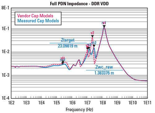
Figure 12. Comparison of the complete PDN impedance as seen by the DDR VDD bumps at the die.
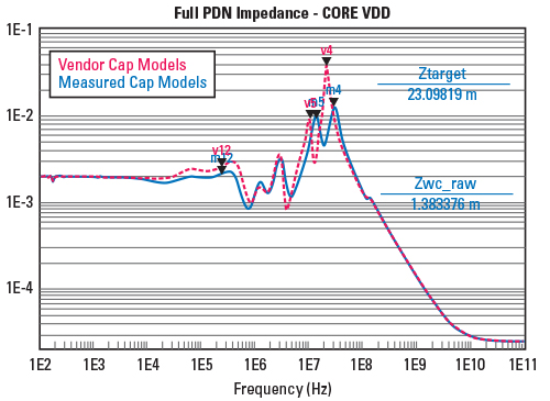
Figure 13. Comparison of the complete PDN impedance as seen by the CORE VDD bumps at the die.
Due to the additional ESL included in the vendor capacitor models, the PDN yields a false additional impedance peak at 21 MHz, as shown by marker v2 in Figure 12 and marker v4 in Figure 13. This peak is 3x greater (about 24 mΩ higher) than the nearest impedance peak at marker m2 in Figure 12 and marker m4 in Figure 13, and exceeds the target impedance. Typically, a PDN designer would try to correct the impedance resonance by adding more capacitance, leading to over-design. Since this impedance peak is not real, by adding more capacitance, designers may inadvertently create sharp anti-resonances, making the PDN unstable.11
Also observed in Figures 12 and 13 is a significant impedance difference at the lower frequencies, as seen at markers vl1 in Figure 12 and vl2 in Figure 13. At 250 kHz, vendor models attribute 296 pH more inductance on the DDR VDD rail and 288 pH more on the CORE VDD rail.
As discussed in Dannan et al.9, initial power integrity analysis happens in the frequency domain. However, design sign-off must occur in the time domain. Figures 14 and 15 demonstrate the time domain voltage ripple results of the Figure 9 simulation, as observed at the die bumps using vendor capacitor models (see Figure 14) and instead using measurement-based capacitor models (see Figure 15).
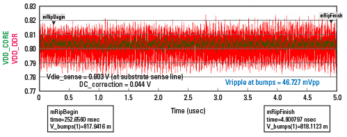
Figure 14. Voltage ripple with vendor capacitor models.

Figure 15. Voltage ripple with measurement-based capacitor models.
These results are summarized in Table 1, which shows a 5.5 mVpp, or 11.77%, greater voltage ripple with vendor capacitor models. This is caused by the false additional PDN impedance peak, which, if trusted, could be the difference between passing or failing an ASIC’s AC voltage compliance specification when using a vector-based dynamic current profile from a die model.
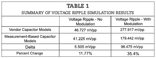
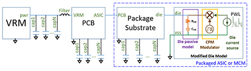
Figure 16. Power integrity system diagram model with modulated CPM.9
As summarized in Table 1, with load current modulation at peaks at m2 and m3 on the VDD_DDR PDN (see Figure 17) and at m4 and m5 on the VDD_CORE PDN (see Figure 18), a 98.47 mVpp, or 35.4%, greater voltage ripple is observed. This shows how harmful the additional ESL in vendor capacitor models can impact time domain simulation results.
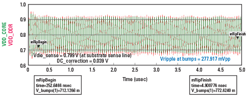
Figure 17. Voltage ripple with vendor-based models and peak modulation.
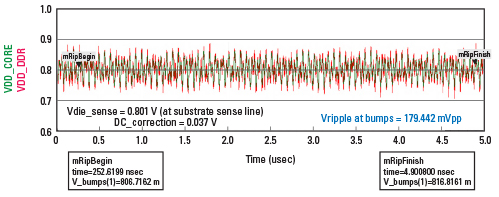
Figure 18. Voltage ripple with measurement-based models and peak modulation.
Conclusion
There is no standard method for de-embedding the measurement mount for capacitor models provided by component vendors. Any capacitor model from a vendor may or may not be de-embedded from the PCB mount. Unfortunately, there is often no way to know if a capacitor model includes the PCB mounting inductance beyond making measurement-based models for that capacitor.
As a call to action, vendors should prioritize the improved accuracy of their capacitor models. A standard is needed or, at minimum, designers need to understand how the vendor model was measured. Doing so will enable designers to create faster and more accurate system models, and vendors can benefit by offering products designers can trust. If Vendor A’s models certify that they are de-embedded from a fixture mount, whereas Vendor B’s models do not specify, a designer will likely select Vendor A’s capacitors as a head start on the design analysis.
De-embedded capacitor models must be used for design analysis. Engineers must make their own using an accurate measurement setup if a vendor cannot provide them. It was shown by using measurements without de-embedding the test fixture (typical of many vendor capacitor models) that additional ESL significantly impacts a PDN design analysis in both the frequency domain and time domain. Additional ESL in a capacitor model can lead a designer to over-design the PDN to address these false impedance peaks. To achieve design sign-off for PDNs, simulations must include accurate capacitor models with the PCB mounting inductance removed. If accurate capacitor models are unavailable, designers should be prepared to make their own measurement-based models.
REFERENCES
- H. Barnes, “Power Integrity Target Impedance Says it All, Power Delivery is AC not DC,” 14th Annual Central PA Center for Signal Integrity Symposium, Harrisburg, 2021, pp. 1-54.
- S. Sandler, “ Why Full VRM Characterization is Essential,” Signal Integrity Journal, 2019.
- S. Sandler, B. Dannan, and H. Barnes, “Partial Inductance – The Secret to Correlating Simulation and Measurement,” EDICON 2022.
- S. Sandler, H. Barnes, and B. Dannan, “CHIPHEADS, Hands-On PDN Impedance and Calibration Basics,” DesignCon, 2023.
- S. M. Sandler, “Extending the Usable Range of the 2-port Shunt through Impedance Measurement,” IEEE MTT-S Latin America Microwave Conference, Dec. 2016, pp. 1–3.
- B. Dannan and S. Sandler, “Calibrating the 2-Port Probe for Low Impedance PDN Measurements,” Signal Integrity Journal, 2021.
- Keysight PathWave PIPro, Web: https://www.keysight.com/us/en/product/W3034E/pathwave-pipro.html.
- P. J. Pupalaikis, ”S-Parameters for Signal Integrity,” Cambridge: Cambridge University Press, 2020.
- B. Dannan, J. Kuszewski, et al., “Improved Methodology to Accurately Perform System Level Power Integrity Analysis Including an ASIC die,” DesignCon, 2022.
- S. Sandler, B. Dannan, H. Barnes, C. Yots, “VRM Modeling and Stability Analysis for the Power Integrity Engineer,” DesignCon, 2023.
- S. Sandler, “Designing Power for Sensitive Circuits,” Signal Integrity Journal, 2017.
- Picotest J2113A Semi-Floating Differential Amplifier, Web: https://www.picotest.com/products_J2113A.html.
- Picotest Omicron Lab Bode 100 VNA, Web: https://www.picotest.com/products_BODE100.html.
- Picotest PDN Cables, Web: https://www.picotest.com/pdn-cable.html.
- Analog Devices LTM4650-2 Dual 25A or Single 50A μModule Regulator, Web: https://www.analog.com/en/products/ltm4650- 2.html.
- Cadence Voltus IC Power Integrity Solution, Web: https://www.cadence.com/en_US/home/tools/digital-design-and-sign- off/silicon-sign-off/voltus-ic-power-integrity-solution.htm