
A common design technique for power distribution networks (PDN) is the determination of the peak distribution bus impedance that will assure that the voltage excursions on the power rail will be maintained within allowable limits, generally referred to as the target impedance. In theory, the allowable target impedance is determined by dividing the tolerable voltage excursion by the maximum change in load current. Measuring in the time domain offers a large signal measurement solution, however, this test method is much more difficult to perform because the ability to control very high speed current steps is challenging, and may not even be possible. The time domain measurement result can also be easily misinterpreted. This article focuses on the fundamental flaw of using target impedance as an assessment method. Using simple, lumped element models and both frequency domain and time domain simulations key issues are highlighted. A high performance optimization simulator (ADS) is used to determine the best- and worst-case voltage excursions for a given tolerance.
Introduction
In a typical high speed application a voltage regulator module (VRM) is connected to the load device (often a field programmable gate array (FPGA) or central processor unit (CPU)) through printed circuit board planes and a multitude of decoupling capacitors. The load device itself presents its own parasitic elements, such as the pin and bond inductance and die capacitance. The result of this distribution network is a series of transmission lines, including the printed circuit board parasitic resistance, inductance, and capacitance. In addition, there are multiple decoupling capacitors, which also present parasitic resistance and inductance elements. It is well known that the lowest noise is the result of a flat impedance response over a very broad frequency range. A typical distribution network is shown in Fig. 1.
The target impedance at the load is generally defined by the relationship between the allowable noise voltage and the maximum variation in the current demand. A major emphasis is placed on the noise due to this load demand in CPU and FPGA applications because this is generally the largest and most significant noise source.

The typical PDN impedance plot is not necessarily as flat as desired. Even in the lower frequency range, many VRMs and point-of-load regulators (POLs) exhibit multiple resonances and anti-resonances rather than the desired flat response (see Fig. 2).
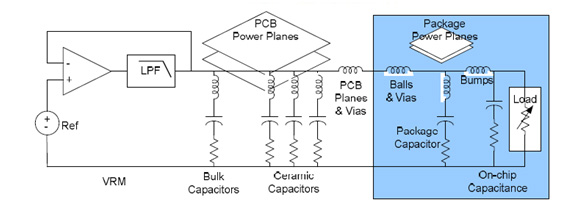
Fig. 1. A schematic diagram of a typical Power Distribution Network (PDN).
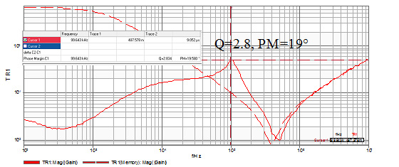
Fig. 2. This low frequency PDN impedance measurement shows that not all PDN impedance profiles are flat.
The mathematical evaluation of the voltage noise induced by a change in current can be easily accessed for a 2nd order distribution network using Laplace and/or Fourier techniques. This simple assessment quickly shows that there are a multitude of possible solutions depending on the nature of the current signal definition and whether the damping of the distribution network anti-resonance is critical, over-damped, or under-damped.
Relating Voltage and Current
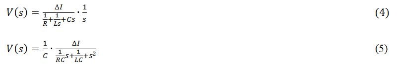
The Laplace solution of the parallel RLC circuit is easily evaluated as a function of the current through each of the R, L, and C elements.

Which can be rearranged to solve for the noise voltage, V:

In the case that the current signal is a unit step of magnitude ΔI, then the Laplace of the current signal is ΔI/s and the voltage can be written as:
In the under-damped case this results in the solution:
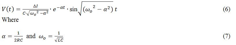
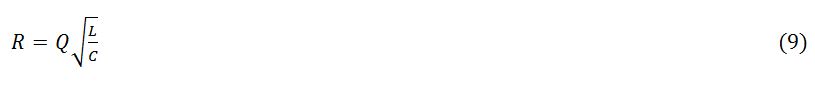
The Q of the parallel RLC circuit is defined as:

Solving for R results in:
Solving for α as a function of Q by substitution:

And finally, we can show that the exponential decay is related to the circuit Q:

If the same circuit is assessed with a sinusoidal current signal at the anti-resonant frequency 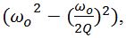 the result takes the form of:

Driving the circuit with a square wave rather than a sine wave results in an amplitude multiplication due to the Fourier coefficient 4/(nπ), causing a 27% larger fundamental amplitude than a sine wave. We have clearly shown that for the under-damped case of a single LCR circuit there are at least three solutions for a constant amplitude envelope, dependent on whether the current signal is a step, sine wave, or square. And so we have now shown that a single current step can result in three different voltages for a given impedance.
A SIMPLE LUMPED ELEMENT EXAMPLE
Using a second-order LCR network simulation model allows a visualization and comparison of the resulting solutions of these three cases. The circuit values are held constant in all three simulation cases. Constraining the current signal to a 0 to 2 Amp envelope allows a direct comparison of the step, sine, and square wave responses. The model schematic is shown in Fig. 3 and the resulting impedance and Q are shown in Fig. 4.
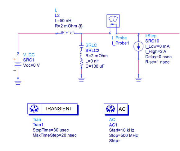
Fig. 3. A simple 2nd order LCR network constructed in Agilent ADS 2011.
The circuit Q can be calculated from the inductance, capacitance and series resistance as:

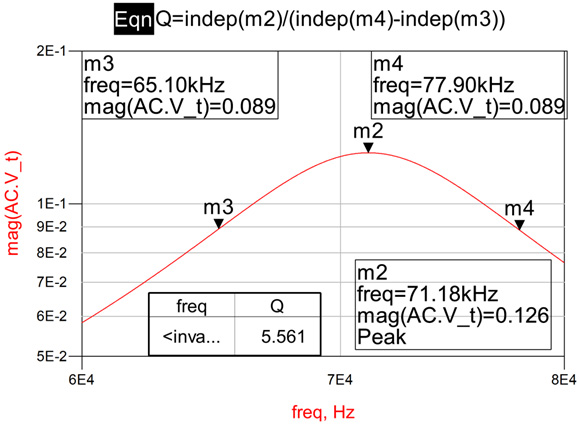
Fig. 4. The peak AC impedance simulation result of the 2nd order LCR network.
The Q can also be determined from the impedance -3dB and center frequencies. The AC simulation result shown in Fig. 4 indicates that the circuit peak impedance is 126 milliOhms with a Q of 5.56 as expected.
This circuit is then simulated using a 2A step, a 2App sine wave, and a 2App square wave current signal source for corroboration of the three expected voltage responses (see Figs. 5, 6, and 7, respectively). In each case, the plot shows both the excitation current and the resulting voltage signal. The sine wave is a pure source; therefore, we expect the time domain response to be equal to the peak impedance if the sine wave is at the exact frequency of the anti-resonance. At frequencies above or below the anti-resonant frequency, the resulting voltage will be smaller, though it will still be a direct reflection of the frequency-dependent network impedance.
Fig. 5 displays the results of applying the 2A step function, which results in a voltage excursion of 43mVpk. As expected, the voltage response is exponentially decaying due to the under-damped solution. This natural response is the smallest excursion of the three solutions.
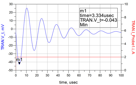
Fig 5. The response to a 0 to 2 Amp step results in a 43mVpk excursion and a damped ringing response as expected for this under-damped case, represented by a Q of 5.56.
In the second simulation the current signal is replaced with a sine wave at the anti-resonant frequency of 71.18 kHz, while maintaining the same envelope limits of 0 to 2A (see Fig. 6). This simulation results in a peak voltage excursion of 124mV, which is very close to what we expected based on a 1A peak excursion and a 126 milliOhm impedance. It is also noted that, as expected, the voltage response exhibits an exponential growth at a rate related to the circuit damping. The circuit requires approximately 6 cycles to reach the maximum steady state amplitude as a result of the resonant Q.
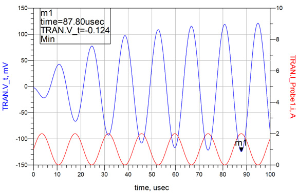
Fig. 6. The response to a 0 to 2Amp sine wave at the anti-resonant frequency results in a 124mVpk excursion and an exponential growth response as expected for this under-damped case, represented by a Q of 5.56. The steady state response for this condition is approximately a factor of 3 greater than the natural response case.
In the third simulation, the sine wave is replaced with a square wave of the same amplitude (see Fig. 7). The result is increased by a factor of 4/(nπ) as represented by the 158mV excursion for the same current envelope of 0 to 2A. The exponential growth is essentially the same as for the sine wave case, requiring 6 cycles to reach the steady state solution.
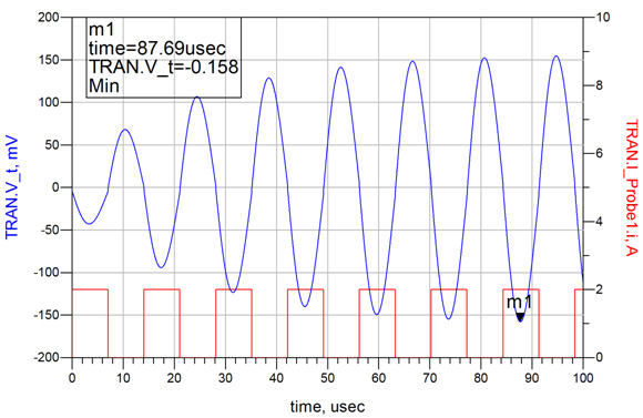
Fig. 7. The response to a 0 to 2Amp square wave at the anti-resonant frequency results in a 158mVpk excursion and an exponential growth response consistent with the sine wave case. The excursion is approximately 27% greater than the sine wave case, consistent with the 4/(nπ) Fourier coefficient multiplier.
To this point we shown mathematically, and confirmed through simulation, that there are three possible solutions for a given current amplitude. In this example, the signal ranges from 43mVpk to 158mVpk, for the same target impedance and depending only on the shape of the current signal. This is clearly a significant limitation of the target impedance assessment method.
Multiple Resonances Can Yield a Rogue Wave
Despite the goal of maintaining a flat impedance profile, a typical distribution network can have many resonances. Some are beyond control, while others are due to non-idealities of decoupling capacitor selection and placement, as well as PCB design tradeoffs.
A few additional elements are added to our simulation model in order to define two additional anti-resonances (see Figs. 8 and 9). These values are not selected based on any particular criteria, but are just spaced over a wide frequency range and adjusted to maintain an under-damped circuit and complying with a 125 milliOhm target impedance.
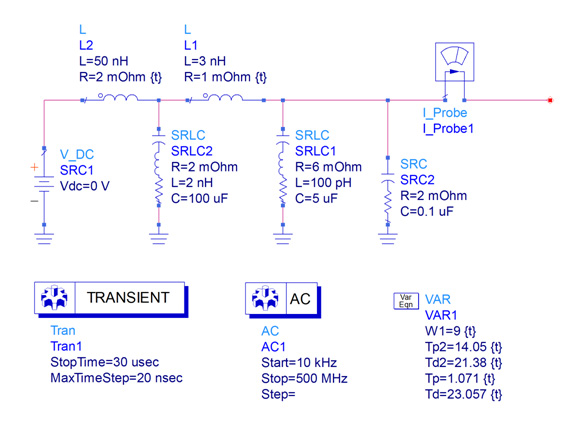
Fig. 8. The simple example circuit is modified to include two additional anti resonances.
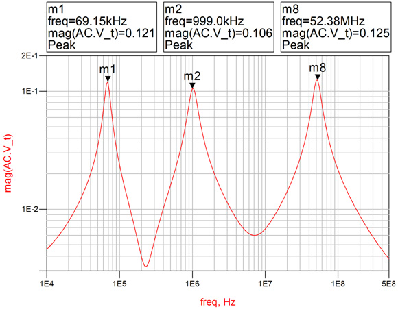
Fig. 9. An AC simulation of the modified example circuit confirms that each of the three anti-resonances is maintained at the desired target impedance of approximately 125 milliOhms.
A load circuit is also constructed in order to allow versatility in the definition of the current signal, which is still maintained within an envelope of 0 to 2 Amps (see Fig. 10). The load circuit contains square current signals at each of the anti-resonant frequencies while also allowing adjustments of the time delays between each current signal application. SRC16 is used to provide the AC current for the impedance measurement. SRC12 is the lowest frequency, while SRC10, SRC11, CRC13, and SCR14 provide the burst for the second frequency and SRC14 provides the third and highest frequency.
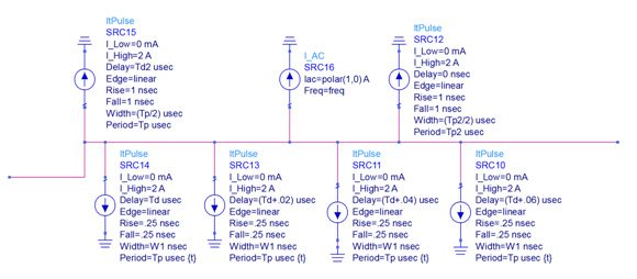
Fig. 10. A time domain load circuit allows application of current signals at any or all of the three anti-resonant frequencies as well as the adjustment of timing associated with the various current signals
The first current signal applied is from SRC12 at the first anti-resonant frequency of 69.15 kHz. The resulting voltage signal shows evidence of the two higher frequencies at the leading edge. At 21.38 uS, the second current signal is applied and the amplitude exponentially increases in accordance with the anti-resonant Q at the second frequency. At 23.057 uS, the third current signal is applied at the third anti-resonant frequency and the voltage excursion associated with this frequency also increases exponentially in accordance with the anti-resonant Q associated with this third frequency. These various signal characteristics are shown in the “zoom” windows in the following simulation plot. The timing for the application of the second and third signal applications is critical and there are three governing criteria.
- The current signals must be maintained within an envelope of 0 to 2 Amps.
- Each signal requires a minimum of cycles to reach steady-state amplitudes.
- The time shift between frequencies is critical, as each of the signal peaks must coincide in time despite the fact that these signals are not correlated or harmonically related.
Each of the three signal source amplitudes are defined as a square wave from 0 to 2 Amps and the timing is manually adjusted to assure that no two independent signals are positive at the same time; In order to keep the current excitation constant only one signal source can be positive at any instant in time.
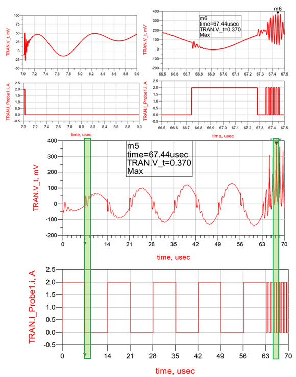
Fig. 11. The nominal simulation results showing the application of the first frequency, as well as, the addition of the other two frequencies. Two zoom views highlight the leading edge ring at the beginning of the simulation and a detailed look at the two additional frequencies.
Based on the simulator results and observations, the approximate PDN noise induced is not limited to the product of the change in current amplitude and the target impedance magnitude, but the product of the summation of the independent impedance peaks and current change products:

where 0 denotes the DC term.
USING THE ADS OPTIMIZER TO DETERMINE A SOLUTION
The Agilent ADS simulator includes many different performance optimizer algorithms and a “cockpit” from which the optimizers can be easily controlled. Each optimizer uses a different combination of error-function (EF) formulation and search methods to achieve a desired goal. In this study, the goal was defined as the maximum (or minimum) excursion resulting from the current signal. The optimizer is an ideal solution as there are many interrelated parameters and it would be very difficult to determine the correct result manually as there are many interdependent parameters.
The steps performed by the optimizer are:
- Perform a simulation using the nominal values for each parameter.
- Compare results with the goal (is it the maximum result) using the combination of error functions associated with the chosen optimizer.
- Modify the circuit parameters within the specified limits to obtain results that are likely to be closer to the goal. Each optimizer uses a different algorithm to find the best solution.
- Perform a new simulation with the modified circuit parameters. This process is repeated up to the maximum allowable number of iterations. If the optimizer does not improve the result for a number of simulations it will return the result without running the maximum number of iterations.
Before using the optimizer at least one goal component needs to be included in the schematic. The goal component establishes the measurement value for optimization and the desired final value for the measurement. The schematic must also include optimization limits for each parameter that can be adjusted and the limits within which that parameter may be adjusted. These limits can be set as absolute limits, percentage limits, or unrestrained limits. An optimizer type must be selected. The Random optimizer is selected and set to allow a maximum of 100 iterations, adjusting each element within the allowed range to achieve a maximum transient voltage excursion. The random optimizer works well when there are many interdependent parameters. The ADS simulation schematic showing the Optimizer functions is shown in Fig. 11.
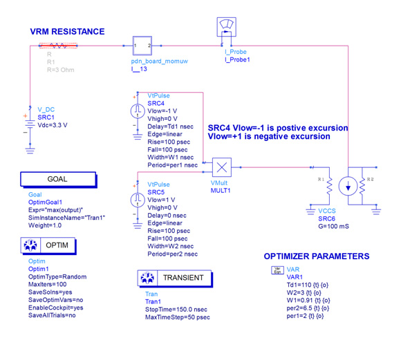
Fig. 11. ADS model of the PCB including the two loading profiles and a random optimizer, used to determine the profile required to achieve the maximum voltage excursion for a fixed current amplitude.
While the Optimizer runs the simulator continually varies parameters in accordance with the chosen algorithm (random in this case). Graphic information, shown in Fig. 12 provides insight into which parameters have the most significant impact and how the output goal (voltage excursion in this case) is changing as parameters are being varied. This particular simulation was performed in less than 1 minute.
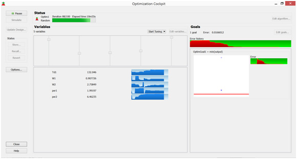
Fig. 12. The graphic Optimizer display, showing the optimizer progress and individual sensitivities. Note in this display the Optimizer variables are no longer changing, indicating that the optimum solution has been identified.
The results of the Optimizer are simulated and the voltage excursion is shown in Fig. 13. It is noted that due to the high Q of the first resonance it takes many cycles to reach maximum amplitude. Once the first resonance as reached maximum amplitude, at approximately 140ns the second current profile is introduced. The excursion from the second current profile is now stacked on top of the first resonance. In this case the resulting excursion is not the sum of the two individual excursions. This is due to the limitation imposed by the number of cycles at the second resonant frequency that can be included in the off time of the first resonance. If the two resonant frequencies were further separated, additional cycles could be included further increasing the voltage excursion. The current profile created by the Optimizer is shown in Fig. 14.
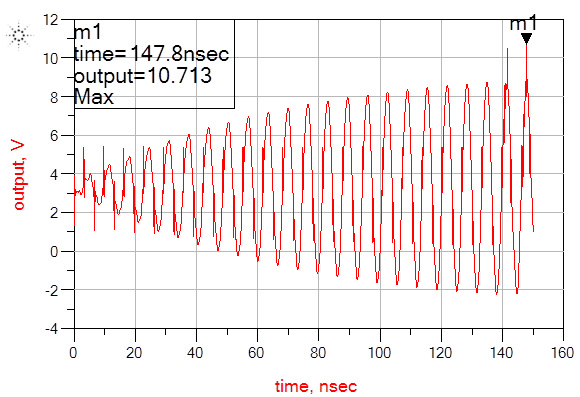
Fig. 13. The voltage excursion resulting from the current profile created by the Optimizer. Note that the second current profile is introduced at approximately 140ns.
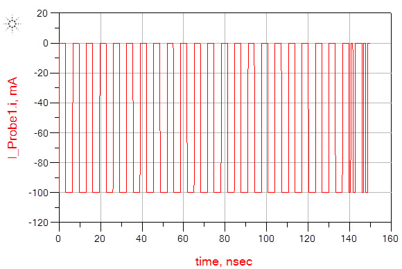
Fig. 14. The current profile created by the optimizer. The second profile is delayed approximately 140ns to allow the first resonance to reach maximum amplitude. The final result is limited by the maximum current step and by the limited number of cycles that fit in the off time of the first resonance.
CONCLUSION
While many publications calculate a maximum acceptable target impedance as the maximum allowable voltage excursion divided by the maximum expected current step, it is shown here that the target impedance assessment has a very weak relationship with the voltage excursion, even for a fixed current step. Several recent publications have introduced the concept of switching patterns and the impact that the switching pattern has on the result. This paper has shown that it is possible for the excursion to reach a maximum level that can be defined as an infinite summation of current impedance products for all harmonics including zero. A mathematical solution to the number of cycles required at each anti-resonance has also been determined in relation to the Q of the anti-resonance.
The optimal assessment method is still impedance; however, the assessment must carefully consider the conditions in which the anti-resonances become additive, as well as the general tendency for the majority of the noise signal to naturally gravitate to the higher frequencies due to the cumulative effect. It has also been shown that the effect of parameter tolerances can significantly impact the noise level and, again, the tolerances tend to skew the noise towards the higher frequencies, also due to the cumulative effect.
This paper was presented at DesignCon 2015.
Author Biography
Steve Sandler has been involved with power system engineering for more than 37 years. Steve is the founder of AEi Systems, a well-established leader in worst case circuit analysis and troubleshooting of satellite and other high reliability systems. He is also the founder of PICOTEST.com, a company specializing in accessories for high performance power system and distributed system testing. He frequently lectures and leads workshops internationally on the topics of power, PDN and distributed systems. Steve Sandler frequently writes articles and books related to power supply and PDN performance.
References
- Om P. Mandhana, “Modeling, analysis and design of resonant free power distribution network for modern microprocessor systems,” IEEE Trans. Advanced Packaging, vol. 27, no. 1, pp. 107-120, Feb. 2004.
- L. Besser and R. Gilmore, Practical Rf circuit design for modern wireless systems: Volume 1 passive circuits and systems, Norwood, MA: Artech Print on Demand, 2003.
- W. Cheng, A. Sarkar, S. Lin, and Z. Zheng, “Worst case switching pattern for core noise analysis,” DesignCon, 2009.
- S. Sun, L. D. Smith, and P. Boyle, “On-chip PDN noise characterization and modeling,” DesignCon, 2010.
- L. D. Smith, S. Sun, P. Boyle, and B. Krsnik, "System power distribution network theory and performance with various noise current stimuli including impacts on chip level timing,” in Proc. Custom Integrated Circuits Conference, San Jose, CA, 2009.
- I. Novak, “Comparison of power distribution network design methods: Bypass capacitor selection based on time domain and frequency domain performances”. Manuscript for TF-MP3 “Comparison of Power Distribution Network Design Methods” at DesignCon 2006, February 6-9, 2006, Santa Clara, CA
- C. K. Cheng “Power Distribution Network Simulation and Analysis” UCSD March, 4, 2010
- Hu, Xiang, Peng Du, and Chung-Kuan Cheng. "Exploring the rogue wave phenomenon in 3D power distribution networks." Electrical Performance of Electronic Packaging and Systems (EPEPS), 2010 IEEE 19th Conference on. IEEE, 2010.