
For a very long time it has been a practice to use the designator “FR-4” to call out a laminate material to be used to fabricate a printed circuit board (PCB). A fair question to ask is "What material does one get in a PCB when FR-4 is the only specification given?"
It turns out that FR-4 is not a materials specification as such. FR-4 stands for an Underwriters Laboratory specification called "Flame Retardant Class 4." This standard specifies that a material will not sustain a flame when it is exposed to heat. It will burn, but, when the heat is removed, the material is self-extinguishing. Originally, this was a safety standard to avoid catastrophic fires in equipment that contains large numbers of printed circuit boards or other items made with organic compounds. Every laminate system available in the U.S. and majority of the rest of the world meets the FR-4 standard. So, if it is the only requirement stated on a fabrication drawing, every fabricator can be in compliance with the specification, but every PCB can be different.
It is fair to ask how the industry came to refer to laminates by only the FR-4 designator. A look at the history of laminate development tells the story. In the early days of PCB manufacturing, there were primarily two choices of laminates: epoxy-based or polyimide. The primary difference between them is their ability to withstand high temperatures. At the melting point of eutectic solder (185°C) the epoxy-based resins become soft and have a very high temperature coefficient of expansion. This requires care when performing wave soldering as well as rework to avoid warping and lifting of the pads. The benefit of epoxy-based systems include ease of lamination and low cost. Where applications required operation or rework at high temperatures, the choice became polyimide. The downsides of using polyimide include the much higher cost and their tendency to absorb moisture to such an extent that PCBs made from them fail leakage tests in humid environments. As a result, conformal coatings are applied.
Based on the foregoing, any design that did not require operating at high temperatures could be made from epoxy-based resin systems. Designers who did not need a high temperature laminate would simply use any laminate system that satisfied the FR-4 standard and focus on ensuring the lowest price possible. The fabricator was free to choose the laminate system and usually picked laminates that were already in stock to minimize turnaround time.
This simple method of specifying laminates worked well as long as the type of laminate had no effect on signal integrity. As electronic speeds have increased into the gigahertz range, the laminate systems can have a devastating effect on performance if not chosen carefully. The two primary negative effects caused by an epoxy-based laminate system are signal loss along the path and skew in a differential pair induced by the choice of glass weave. Simply asking for a material called “FR-4” will no longer work.
The current state of electronic design can be divided into two major classes: designs that are slow enough that the choice of laminate system has little effect on operation or reliability, and those with operating frequencies high enough that laminate choice can have an adverse effect on performance.
A better way to specify the laminate system of choice for the former is Standard Commercially Available Laminate (SCAL) and for the latter, Low Loss Laminate (LLL). In fact, just specifying low loss laminate for high-performance designs is still not enough to assure proper operation. It is necessary to specify the resin system that will result in acceptable loss in the signal paths, along with the exact glass weave style that will be used next to any signal layers to minimize unwanted skew.
Figure 1 is a stackup drawing showing the minimum information needed to describe a PCB that is intended for multigigabit operation. This stackup is for a PCB that has dozens of 28 Gbps serial links on it and 29 different power rails, one of which is 120A at 0.9V.
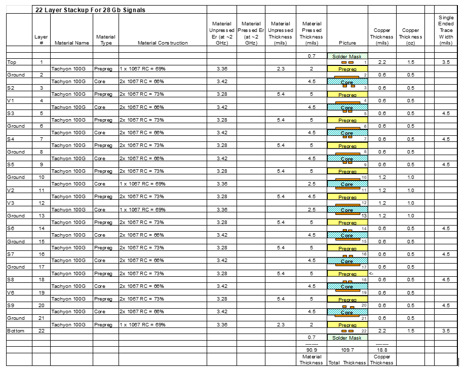 Figure 1. 22-layer PCB stackup for a design with hundreds of 28 Gbps serial links.
 In Figure 1, it is important to note that the third column from the left calls out the laminate system to be used, while the fifth column calls out exactly what glass weave styles to use in each layer of the PCB. Calling out the laminate system is intended to ensure that the path losses are within design limits. Calling out the glass weave style is intended to minimize glass weave-induced skew in differential pairs. As performance frequencies continue to increase, the need to be this specific becomes more important. For example, version 4 and higher of PCIExpress requires this level of control over materials.
When the goal is the lowest possible overall loss, an unapparent source of loss is the roughness of the copper foil used in the signal and power layers. For a very long time, the default copper foil finish in PCB laminates has been a finish called Reverse Treat (RTF) copper. This finish was engineered to ensure good adhesion of the resin in the laminate system to the copper during lamination. If no surface finish is specified, the copper finish in nearly all PCBs will be RTF copper. RTF copper results in significant loss at very high data rates.
When the aim is to achieve the lowest possible loss, the copper finish used is often called Very Low Profile (VLP) copper.
Figure 2 illustrates the difference between the two types of surface finishes. On the left is copper foil manufactured with RTF copper, and on the right is copper foil manufactured with VLP copper. It is clear that the VLP copper is much smoother than the RTF copper. This will have a measurable effect on loss at very high data rates.
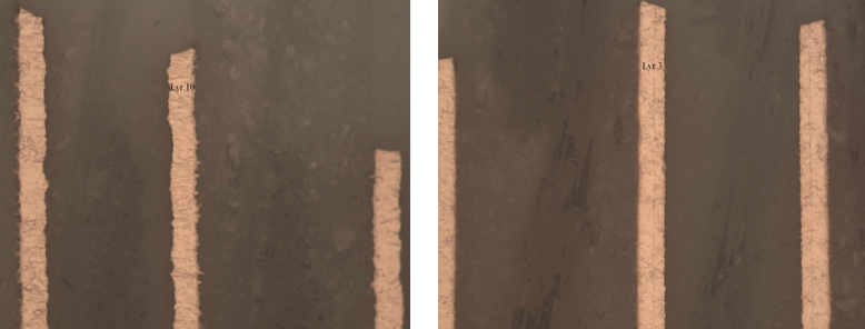 Figure 2. Cross section of two identical PCBs, one using RTF copper (left) and one using VLP copper (right).
Another unapparent source of loss at high data rates is the finish applied by the fabricator to the copper surfaces that contain traces and their corresponding plane layers. For a very long time, the fabrication industry has applied a finish to all exposed copper known as brown or black oxide. This is done in order to increase the roughness of the copper to promote good adhesion during lamination.
Figure 3 contains two cross sections of two PCBs fabricated from the same material and the same artwork at two different factories. The upper surface in both sections is the side of the copper that the fabricator treated to promote adhesion during lamination. The section on the left was treated with an adhesion promoter called Atotech Bondfilm, whereas the one on the right was treated with brown oxide.
The measured path loss for the PCB on the left was 37 db at 8 GHz, and the on the right, the measured path loss was 40 db at 8 GHz. The 3 db of difference is attributable to the surface finish applied at the fabricator. For today’s high-speed and high-data rate designs, this difference can mean the difference between a PCB that will operate correctly and one that will not satisfy the high-speed criteria.
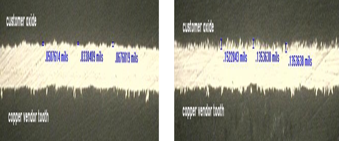 Figure 3. Two cross sections of the same PCB fabricated in two different factories.
The above discussion illustrates the need to include more control over what copper finish is used in the laminate and what copper finish is applied by the fabricator.
There are two fabrication notes that specify both of these parameters:
- All signal and power layer copper finish should be VLP or HVLP copper foil
- Fabricator applies finishes to internal signal and plane layers to be Atotech Bondfilm( or equivalent), which does not degrade the VLP or HVLP copper surface finish.
Summary
Within the PCB industry, FR-4 materials have long been accepted as “standard” materials. However, their use was not specific to the types of board being designed. For today’s high-speed, high-frequency designs, careful engineering and material selection relative to the resin systems and glass weave styles needed will ensure that a product will work as specified, as designed and as manufactured. In addition, the finish of the copper used in the signal and power layers also needs to be controlled in order to ensure that loss goals are met.