
There is a general understanding that the amount of jitter or time interval error (TIE) observed at the output of a lossy or reflective channel is larger than jitter or TIE of the transmitted signal. Even with an ideally clocked input signal, TIE in the output waveform can appear as jitter in the eye diagram. But what exactly happens if input jitter is increased by a certain value, such as a fraction of the unit interval (UI)? Will the output jitter increase by the same amount or more?
It turns out that in most cases an increment of the input jitter by a certain fraction of the UI (while keeping its distribution and spectral properties unchanged) makes the output jitter increase by a larger amount. This effect is called “jitter amplification.” It has been known for decades and studied in numerous publications.1-4 Still, this phenomenon remains somewhat of a mystery, because it lacks a general and simple explanation.
Some people believe that jitter propagation through a channel can be studied in the same way as propagation of voltage, current, or waves. If so, the problem can be solved by finding a jitter propagation or transfer function to greatly simplify jitter study, prediction, and possibly, mitigation. Indeed, such characteristics are found for some channels, and specific jitter properties, mostly assuming small jitter magnitude and/or certain types of distribution, spectral, and correlation properties. Unfortunately, no general solution exists because jitter propagation cannot be described by a linear transfer function, even for a perfectly linear time invariant channel.
There are some fundamental reasons why. Most importantly, jitter is not a physical parameter directly associated with energy possessed by a physical system. Unlike jitter, the voltages, currents, or scattering parameters measured at the ports of an electrical circuit are directly related to the power that comes in or out and, therefore, the power that is stored or dissipated in the system.
As power-related parameters, they obey several conservation laws, such as Kirchhoff’s current and voltage laws. These laws, together with component relationships (Ohm’s law) make it possible to superimpose the values of these physical parameters in linear circuits. However, no similar reasoning applies to jitter. For example, doubling the peak-to-peak or RMS value of jitter at the input does not necessarily translate to a doubling at the output; and, the combination of two jitter types does not necessarily produce the sum of their separate effects.
Our goal is not to find a jitter transfer function (even if it is possible in some cases), but to think about jitter propagation as a combination of at least two transformations. First, input jitter, a timing variation of the transition, creates vertical “noise” which can be found as the difference between the displaced and non-displaced transitions. Depending on jitter type, this noise could be deterministic or random. Then, the vertical noise at the channel’s input (in a form of a voltage, current, or scattering wave) propagates toward the receiver where it converts back into timing variation or output jitter.
The diversity of jitter types, wide multiplicity of digital signals and variety of different channel characteristics make a unified consideration of jitter propagation impossible. This article starts from the simplest and most popular case of a meander input with duty cycle distortion, illustrating the traditional method and the study of jitter-to-noise and noise-to-jitter transformations. Then, the propagation of small uncorrelated Gaussian jitter is considered. Finally, a general approach is described that applies to large magnitude jitter interacting with an irregular or random input pattern in a lossy channel.
Periodic Clock Signal and Duty Cycle Distortion
This is the simplest and most frequently used example to illustrate jitter propagation because the channel’s input and output are deterministic periodic signals. The input signal is a periodic meander input with symbol interval ![]() and period
and period
![]() The blue waveform in Figure 1 illustrates an undistorted meander with a duty cycle ratio (DCR) of 0.5; the red one has a
The blue waveform in Figure 1 illustrates an undistorted meander with a duty cycle ratio (DCR) of 0.5; the red one has a ![]()
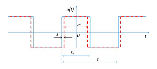 Fig. 1 Periodic meander input with duty cycle distortion.
For any single transition, the timing delta is: 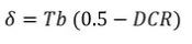
A positive delta creates positive delay for the rising transition and negative for the falling. With the DCR > 0.5, the sign of delta is negative thus reversing the signs of transition delays as well.
What is seen at the output of lossy channels? Consider two channels, providing respectively 3 and 6 dB of loss at the Nyquist frequency with matched terminations (see Figure 2). The output waveforms and eye diagrams are shown in Figure 3.

Fig. 2 Channel transfer functions representing 3 (blue) and 6 (red) dB of loss at the Nyquist
Fig. 3 Output waveforms (a) and eye diagrams (b) with an undistorted input (DCR = 0.5). Similarly, output waveforms (c) and eye diagrams (d) for a moderately distorted input (DCR = 0.45).
In both cases, the DCR is measured at the channel output as a portion of the UI where the periodic signal is positive. This value can be easily expressed via the TIE; or, it can be thought of as a DCR of the digital signal restored from the output waveform by amplification and clamping. Evidently, undistorted input meander creates an attenuated output with the DCR = 0.5 regardless of the channel loss, see Figures 3a and b. With a non-ideal input, however, distortion increases in the lossy channel, and to a larger extent when the loss is higher. This seen in Figures 3c and d. Vertical asymmetry of the eye diagram is also observed when comparing Figures 3b and d. In general, such asymmetry always appears when timing or magnitude distortion is correlated with the digital pattern itself.
What happens if channel loss is increased, or the input DCR is different? This is shown in Figure 4, where each curve corresponds to a certain DCR value at the channel’s input. Distortion increases with channel loss and grows faster with greater input distortion.
 Fig. 4 DCR of the output signal as a function of channel loss at the Nyquist frequency.
Why does the DCR (or peak jitter value) change in the lossy channel. This is explored in two different ways:
- By analyzing the signal spectrum. Since the input is periodic in time, it can be represented by a Fourier series. By multiplying the magnitudes of the spectral components with the corresponding complex values of the channel’s transfer function, the discrete spectrum of the output signal (which is also periodic) is found. The output waveform is recovered by converting the discrete spectrum back into time domain.
- By considering the problem in time domain. For this purpose, the output signal is represented by a combination of the channel’s step responses with different signs and delays.
Explaining Jitter Amplification in the Frequency Domain
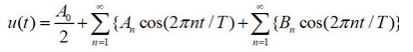
A periodic time domain function can be represented by a Fourier series of the form:

Where:
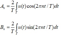
By selecting integration limits symmetrical in time ![]() all coefficients are
all coefficients are ![]() zero and only the cosine components with real magnitudes remain:
zero and only the cosine components with real magnitudes remain:
Magnitudes of the harmonics are shown in Figure 5. For the ideal input (DCR = 0.5) the DC component ![]() and the magnitudes of all even harmonics are zero because
and the magnitudes of all even harmonics are zero because
equals which is identical zero for even.

Fig. 5 The spectrum of the ideal meander with the DCR = 0.5 (blue), and distorted meander with the DCR = 0.45 (red). The ideal meander has no even harmonics nor DC in its spectrum. The distorted meander input has non-zero DC and all harmonics.
The output spectrum can be found by multiplying the magnitudes of the input harmonics with the channel transfer function at the corresponding frequencies. The transfer characteristic of a lossy channel is a complex valued function, so the resulted harmonics are complex as well. For convenience, Figure 6 shows their absolute values.


Fig. 6 Output signal spectrum. Channel with 3 dB loss (a) and 6 dB loss at the Nyquist frequency (b).
Figure 6 provides enough data to explain why the DCR (or jitter) is increased by a lossy channel. Note that duty cycle distortion creates a non-zero DC component in the input signal. This can be seen in Figures 5 and 6. The variable part of the signal is defined by its harmonics starting from the first and above. The lossy channel attenuates the signal at higher frequencies but does not significantly affect the DC component.
For example, in the input meander the ratio of the magnitude of the first harmonic to DC is almost 13, but it reduces to 9 and 6.5 respectively by the channels in Figures 6 a and b. Higher harmonics are attenuated more because the channel loss increases with frequency. If higher harmonics are neglected, the output signal becomes a sine function offset by the DC value. No zero crossing is possible if the magnitude of sine wave is below the DC value, but duty cycle distortion can be enormously large even if the DC value is exceeded by just a small amount.
In a nutshell, “jitter amplification” happens in two stages. First, input timing jitter (in this case, duty cycle distortion) is converted into “vertical noise,” which for the given example is a non-zero DC offset. Then, at the output of the channel this DC offset moves a considerably attenuated “signal” up or down and converts it into a much larger timing variation (output jitter). Both conversions (timing variations into vertical noise and back) are non-linear transformations. Figure 4 illustrates this. In some cases, linearization around a chosen operating point is possible, which provides some insight into the nature of the jitter transfer function. However, in general, such linearized models suffer from inaccuracy and, if applied incorrectly, may lead to large inaccuracies.
Download and read the entire article.