
While the physical design and manufacture of electronic systems has advanced significantly over the years, changes in dimensions and density in printed circuit boards (PCBs) have been incremental – particularly compared to the exponential increase in integrated circuit (IC) density and system interconnect data rates. Indeed, in the past 30 years IC density has increased 100,000x while PCB density has increased 3x [1, page19]. As such, a challenging convergence of operating frequencies and standard PCB dimensions looms on the horizon. For example, although effort is made to keep 28+ Gbps via stub lengths less than 5 mils, few recognize the surface mount pad stub extending beyond the backside of soldered connector pins is often significantly longer than 5 mils.
Of particular concern and focus in this paper is the placement of ground return vias (GRVs) near signal vias. For decades hardware and layout engineers have added GRVs near signal via layer transitions based on best practices, folklore, and fear with little understanding of where GRVs need to be and why. Mystery and misunderstanding have led to re-routes and wasted PCB real estate. As data rates continue to increase, driving significant spectral content into the 40GHz to 60GHz region, it will become ever more important and difficult to place these GRVs where they will get the job done. The goal of this paper is to describe the role and behavior of GRVs in a way that informs design and layout engineers’ intuition and engineering judgement, using practical examples.
Figure 1 shows eight single ended signals under a 1 mm pitch ball-grid array with equivalent ~100 mil vias to the route layer shown, next to measured data for the same. Each of the eight signal vias is immediately surrounded by four GRVs. However the pattern of the GRVs varies, depending on where each signal falls within an alternating 2 mm array of GRVs. The GRVs in the sites labeled “diamond” are closer to their associated signal via (1 mm) than the GRVs in the sites labeled “square” are to their associated signal via (1.4 mm). Measured data (at right) reveals the “square” signal’s insertion loss (IL) decreases to -40 dB at 40 GHz while the “diamond” signal’s IL continues to decrease linearly. How is it possible, simply due to ground via placement, that 99% of the signal is lost for half of the signals while IL for the other half is well-behaved? Furthermore, how can a tiny 100-mil via structure within the same dielectric material exhibit more loss than fifteen inches of trace? This paper will demonstrate the answers lie in understanding the interactions of the via’s return currents.
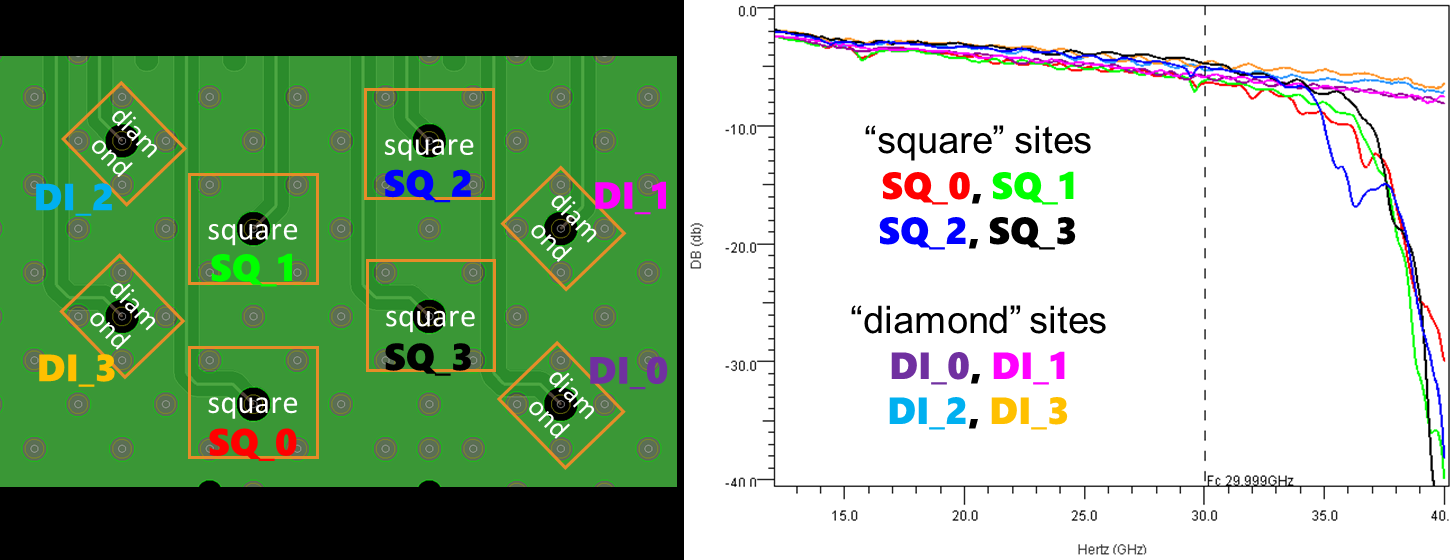
Figure 1: PCB test structure and resulting signal IL
This paper will demonstrate what happens when GRVs are too distant for the data rate at hand. When the distance from the signal via to the GRVs in Figure 1 becomes greater than approximately a quarter wavelength, the structure resonates with a relatively high Q. It is in effect a microwave filter. To help avoid the excessive IL shown in Figure 1, this paper will define a Gap-Rate Distance (GRD) metric that can be easily applied to GRV placement in a PCB layout.
We will use three metrics in both simulation and measurement to gauge the efficacy of passive interconnects as influenced by GRV placement: IL, time domain reflectometry (TDR), and crosstalk. While IL currently gets the most attention because it both reduces the signal amplitude and is a major source of intersymbol interference, SerDes equalization schemes and lower-loss materials have been effective at mitigating IL effects. However, as the authors have been asserting for a long time [2, 3, 4], transmission path discontinuities, as measured by TDR, are every bit as serious a source of intersymbol interference, and significantly more difficult to equalize. Indeed, as increasing miniaturization impacts electronic products, discontinuities are becoming the primary cause of link failure [1, Chapter 4].
Measured TDR in Figure 2 demonstrate that the GRV placements that affect IL in Figure 1 also cause unexpected discontinuities in the transmission path. For ~15 ps, a perturbation relevant to current data rates, the signal via impedance is consistently five ohms higher for the “square” sites than the “diamond” sites. Although one such increase in via impedance might not be a serious problem, multiple irregular vias along a transmission path can cause serious impairments.

Figure 2: Measured TDR for eight test signal vias
Finally, as the measured data and model results in this paper will show, crosstalk is going to become a serious impairment as data rates increase. As shown in Figure 3, measurements demonstrate that at higher frequencies crosstalk between the “square” sites (gold) is higher than the crosstalk between a “square” site and a “diamond” site (blue), which in turn is higher than crosstalk between two “diamond” sites (black). Crosstalk increases rapidly with frequency and is primarily a function of GRV configuration. Note also from the layout that the signal vias are not at all “close” to each other compared to crosstalk dimensions normally considered, indicating some effect beyond capacitive coupling is at work, as will be demonstrated. Although differential transmission improves the situation somewhat, a similar phenomenon occurs for that case as well.
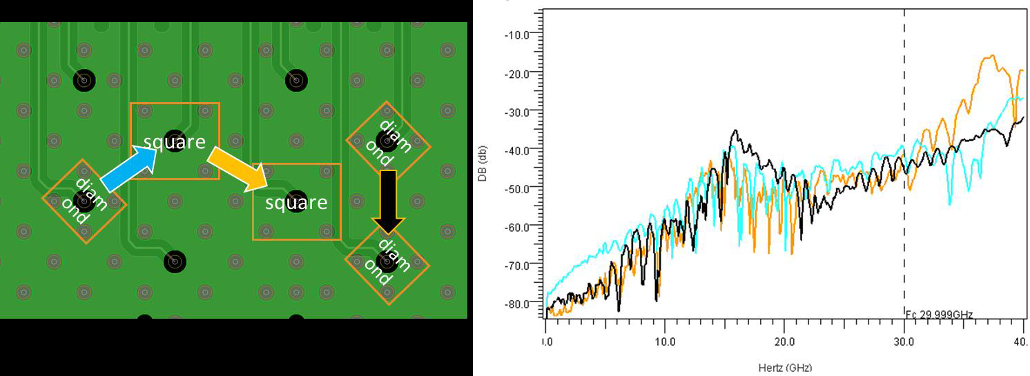
Figure 3: Measured crosstalk for signal vias
This paper is a natural extension of the authors’ compute-efficient and structure-based approach to via modeling [5, 6, 8] to include effects of higher frequencies. While many current applications use differential transmission, this paper will concentrate on single-ended transmission because the role of the GRV is simpler to illustrate and comprehend. However, we will briefly address differential transmission in section 7.1 near the end of the paper.
The paper referenced here received the Best Paper Award at DesignCon 2022. To read the entire DesignCon 2022 paper, download the PDF.