
A key component pushing the success of electric mobility is the vehicle’s traction battery and its functional safety. It is important to monitor the entire battery stack as well as every single lithium (Li) ion cell because the rough environment in an electric vehicle can cause failures that need to be detected very fast. Relevant stress factors are vibrations, mechanical shocks, high currents and extreme temperatures. The cells are therefore supervised regarding their voltage, current, temperature and impedance, which is part of the battery management system (BMS). Using electrochemical impedance spectroscopy (EIS), the cell’s complex impedance value over frequency is a good measure for the internal cell temperature, the state of charge (SoC) and the state of health (SoH). Moreover, comparing the battery stack impedance with the single cell impedances can reveal upcoming high contact resistances.
Single cell monitoring needs to be performed physically close the cell to mitigate impedance measurement errors. Hence, the supervisory electronics needs to be placed as close to the cell as possible. Since the traction battery consists of hundreds of single cells and the monitoring data has to be transmitted to a central electric control unit (ECU) for processing, a huge amount of communication bus wiring is necessary. An alternative to the usually implemented daisy-chain bus system [1] is the approach to send high-speed communication signals directly over the battery chain. This attractive solution would not need any additional wires, as the batteries are used as the communication channel.
To answer the question, whether this novel approach is feasible or not, we need to know more about the high frequency behavior of Li-ion cells. There is very little published on this topic, since up to now only frequencies below 10 kHz were regarded, for example in the EIS since electrochemical processes do not occur faster [2]. However, transmitting the monitoring data of all cells in fixed time intervals requires at least a data rate of 1 Mbit/s. To predict the cell’s performance at such high data rates, a high bandwidth electric equivalent circuit (EEC) model is needed.

Cell Characterization Setup
The first step to obtain an EEC model is to characterize the cell. We have done that by measuring the cell’s impedance up to 300 MHz using the shunt-through 2-port VNA method [3]. This method is very suitable for low impedance values [4], which is the case for battery cells. As depicted in Figure 1, port 1 serves as a current source and port 2 senses the voltage across the cell. Since the cell is very low ohmic, most of the incident signal power will be reflected back to port 1 leading to an S11 close to negative one. A small portion of the signal will be transmitted to port 2 and gives valuable information about the cell’s impedance according to

with the characteristic impedance Z0, which is 50 Ω in our case. The DC blocks in Figure 1 are added to prevent DC currents from flowing into the VNA ports.
A challenge is the connection of the battery cell with the SMA connector based VNA. The connection has to be mechanically as well as electrically stable, so that calibration procedures can be applied. For that purpose, we designed a two-layer printed circuit board (PCB) fixture to mount the battery, which is illustrated in Figure 2. The board has two microstrip lines on the top layer connecting the positive battery terminal with the SMA’s inner conductors and a signal return plane on the bottom layer, which connects the negative cell terminal with the SMA’s signal return conductor. The SMA plugs are connected to the VNA ports via the DC blocks. The cell itself is placed in the cutout of the PCB and the contacts are soldered.
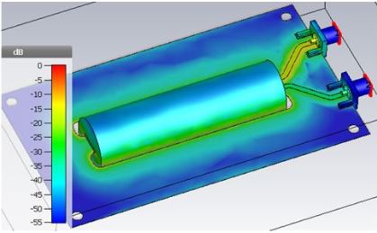
Fig. 2. Normalized current distribution on the fixture for 100 MHz excitation at the upper port3.
The current distribution on the board was simulated using CST Microwave Studio ® and is shown in Figure 2. The current density is highest at the edges of the PCB’s cutout, thus creating the lowest loop inductance.
De-embedding the Cell Impedance
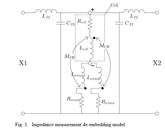
After SOLT (short, open, load, thru) calibrating the VNA, the measurement reference plane is located at the two SMA plugs X1 and X2 of the fixture. Using this configuration, an impedance measurement will result in a “loop impedance” of the fixture and the cell together. The de-embedding model in Figure 3 shows how this loop impedance is composed. It contains the resistance Rcell and the self-partial inductance Lcell, which model the cell for the de-embedding procedure with sufficient accuracy. Furthermore, it contains the signal return path, which is modelled by the resistance Rreturn and the self-partial inductance Lcreturn and is inserted twice because the current can return to either the right or the left around the cell. The mutual inductances MCR account for the inductive coupling between the cell and the signal return path [5] and the elements LTL and CTL model the transmission lines. The transmission lines are compensated by the VNA-provided port extension procedures. Thus, the resulting effectively measured loop impedance derived from Figure 3 is

To remove the fixture’s impact on the measurement results, the cell’s impedance has to be de-embedded from (2). This is obtained by deducting the parasitic fixture effects modelled by Rreturn, Lcreturn and MCR from (2). As we do not know the exact values of these elements, we realized the de-embedding by measuring an analytically known reference impedance, which is a solid copper cylinder with the same dimensions as the cell. The second measurement will have the same parasitic elements, thus the subtraction of the two measurement results Zloop1 and Zloop2 from each other will cancel out the parasitic elements according to

As can be seen from (3), we need to know the resistance RCu and the self-partial inductance LCu of the copper cylinder,
which can be analytically calculated from formulas or simulated using a 3D EM simulator. Of course, the skin effect is considered in these elements, which are therefore frequency dependent. At low frequencies, the measured impedance of the copper cylinder was significantly higher than the 3D-simulated impedance indicating sheath currents. This measurement deviation could be eliminated by encompassing the coaxial cables with ferrit cores.
Impedance Measurement Results and Conclusion
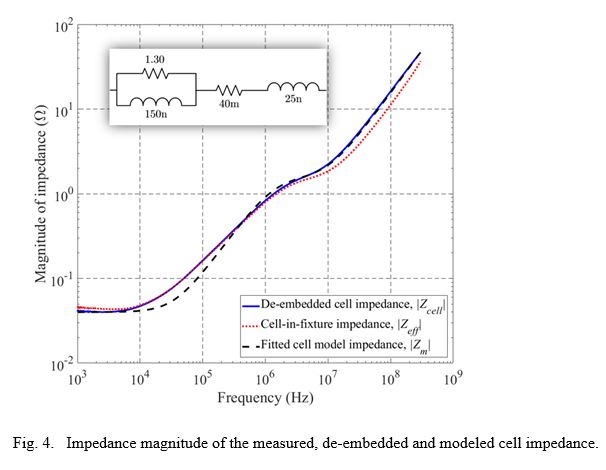
Both the cell and the copper cylinder were mounted on the fixture and characterized using the presented 2-port VNA method. The results of both the in-fixture and the de-embedded cell impedance are depicted in Figure 4. In addition, a simple EEC model is fitted to the de-embedded results using the least square (LS) fitting method. For low frequencies, the cell’s impedance is as low as 40 mΩ but increases up to 40 Ω for high frequencies mainly due to its inductive reactance. Hence, even though a battery is considered to be very low ohmic, at high frequencies we will face less problems on sending high-speed signals over a chain of batteries since its inherently inductive behavior creates a reasonably high impedance. Regardless of these results, the main concern about the data transmission over the battery power line is its electromagnetic compatibility, which is twofold: First, the communication is highly susceptible to impulsive noise generated by the power electronics. This may be overcome by using spread spectrum techniques such as frequency hopping. Second, the communication tends to create additional electromagnetic radiation that may violate legal limits, as the battery pack is not always shielded. These concerns need to be investigated further in future work.
References
- Hong, H., Sevillano, J., Kain, C., Hofer, G. et al., "Alternatives in Battery Communication Protocols," SAE Technical Paper 2017-01-1212, 2017.
- E. Barsoukov and J. R. Macdonald, Eds., “Impedance Spectroscopy: Theory, Experiment, and Applications,” John Wiley & Sons Inc., Hoboken, New Jersey, 2005.
- T. F. Landinger, G. Schwarzberger and A. Jossen, "A Novel Method for High Frequency Battery Impedance Measurements," 2019 IEEE Symposium on Electromagnetic Compatibility, Signal Integrity and Power Integrity (EMC, SI & PI), New Orleans, LA, 2019, pp. 106-110.
- Keysight Technologies, Appl. Note 5991-0213EN, pp. 1‑17.
- C. L. Holloway and E. F. Kuester, "Net and partial inductance of a microstrip ground plane," in IEEE Transactions on Electromagnetic Compatibility, vol. 40, no. 1, pp. 33-46, Feb. 1998.