
Over the past two decades I’ve accumulated a checklist of items required for successful serial link implementation. This list is now boiled down to the “7 Steps to Successful Serial Links” that I teach in my classes, and offer as chapter two in my new book. This article will cover the first two steps: (one) minimize discontinuities, and (two) manage loss. These two steps are the most important, and so we begin here. In fact, all seven steps work together throughout a design and implementation cycle to manage these two challenges from different angles – with or without simulation.
Step 1: Minimize Discontinuities
This is where you need to think creatively. In short, all unnecessary vias, connectors, breakouts, capacitors, traces, cables, and other interconnects should be removed. Why? Because every transition through a new type of interconnect represents another potential “discontinuity,” or element in the connection that can cause an impedance change. Impedance changes cause signal reflections which degrade and distort a signal’s integrity. In fact, discontinuities are the primary cause of link failure, so this is where we begin.
It’s not that discontinuities cannot be managed. It’s just that in the larger realm of manufacturing variables and tolerances, the fewer of them you need to manage the better. Learn to look at the link from end to end, find every place the interconnect transitions, and then remove as many transitions as possible. This is the first and best way to minimize discontinuities: decrease the number in the design phase before you’re forced to control them during implementation.
If your PCB requires the link to go from one device to another device or connector, you should be able to reduce each diff-pair’s complexity to a stripline trace with vias on each end, with perhaps a short breakout trace on one end (which is potentially another discontinuity). Some link protocols allow you to swap p and n in your diff-pair to avoid additional vias. Whatever the case, don’t accept a discontinuity unless it is absolutely required.
Once you’ve removed the unnecessary discontinuities, it’s time to match the impedance of the discontinuities that remain. First learn the impedance of your Tx, Rx, any necessary connector(s), and the impedance specified by the standard or protocol you are using. Then minimize the magnitude of impedance changes along the signal path by intentionally adjusting the impedances when possible.
This normally means using field solvers to calculate and adapt the impedance of traces and vias that are of a relevant feature size [1] for your data rate. Via impedance [2] can be tricky to resolve because via solvers are not as readily available as trace solvers [3]. However here’s a free software trial of Signal Integrity Toolbox with a via solver you can use.
Even when you’ve removed as many discontinuities as possible and matched impedances in your implementation, the manufactured impedance of items you expected to have consistent impedance may not turn out that way. Figure 1 is a TDR [4] of a 6.6 in. trace with two vias and an AC capacitor; the minimum number of discontinuities required for this connection.
As shown, even though the AC capacitor and its associated pads are well-managed, nuances in the routing and PCB construction cause substantial variations from the intended 100 Ohm impedance. This scenario is explained in more detail in reference five (page 14), and reveals that discontinuities may exist even though you removed as many as possible. Which brings us back to where we started: remove all unnecessary discontinuities.

Figure 1. Measured Discontinuities
Step 2: Manage Loss
Loss happens, so the challenge is managing and containing it to an acceptable level. What’s “acceptable” varies dramatically depending on your data rate, protocol, and devices involved. So, the first step in managing loss is to define a loss budget for your link at the frequencies of interest. This may come from your device’s published design guidelines, the serial standard in use, rules-of-thumb, SerDes equalization capabilities, or previous projects.
Table 1 shows a sample “insertion loss” (IL) budget for a 16 Gbps system-level link that spans three PCBs. The good thing about IL is that when discontinuities are decently handled (see step one) it can be summed linearly as shown. 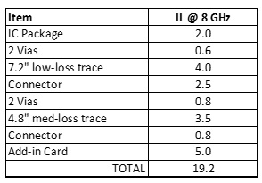
Table 1. Sample 16 Gbps Loss Budget
In the early days of serial links, loss garnered all the attention. As such, SerDes equalization is much better at handling loss than discontinuities. Then numerous low-loss dielectrics appeared, and they are now common and affordable. This led to over-compensation, particularly on short links that didn’t have enough minimum loss to dampen the inevitable reflections caused by discontinuities. Newer serial standards now specify a range for acceptable loss, and it’s a good idea to have a loss budget with both min and max values.
Once your loss budget is known, estimate the loss for all your links. Do not convert loss to length until you understand your trace construction and materials. The most relevant parameters are loss tangent (Lt, sometimes referred to as dissipation factor or Df) and trace width (Tw), which directly correlate to dielectric loss and conductor loss, respectively. If cables are involved, they typically have less loss per inch than PCB traces, as specified in their datasheets.
To illustrate the relevance of trace construction, Figure 2 shows a 3x change in IL at 7.5 GHz for 12 in. of differential PCB trace depending on the materials used. Because loss tangents for PCB dielectrics are available through a 10x range (red=0.002, blue=0.006, green=0.01, gold=0.015, black=0.02), dielectric loss is the dominant effect responsible for the ~3x variation in loss.

Figure 2. 15 Gbps Differential IL Variation for 12 in. of PCB Trace (plot created in MATLAB and Signal Integrity Toolbox™)
Within each Lt value/color in Figure 2, the widths of the differential traces (Tw) are varied from 3 to 9 mils in 1 mil increments. This, in itself, causes more than 1 dB variation in loss at 7.5 GHz due to conductor loss. Widening from 3 to 5 mils significantly reduces conductor loss, while widening beyond 6 mils has less impact.
Figure 2 shows that a 15 Gbps signal might see anywhere from 1/3 dB per inch to 1 dB per inch, depending on how the PCB traces are implemented. That means if your trace loss budget is 15 dB, your max trace length might be anywhere from 15 in. to 45 in. This huge difference illustrates that it is useless to talk about trace length limits until you determine trace construction. Or, looking at it another way, if the length you need has too much loss, it’s possible a change in materials will solve the problem.
Once you know the dB/inch of your trace construction, you will also want to add in loss for any connectors and vias in the path. If you do not know the loss for these items, a rough rule-of-thumb below 10 Gbps is to add 0.5 dB for larger ones (e.g., thick backplane vias, right-angle connectors) and 0.25 dB for smaller ones (e.g., 60 mil thick PCB vias, LGA connectors). If you’re above 10 Gbps, double those numbers.
While this section has focused on managing IL, or how much a signal is attenuated as it travels from Tx to Rx), you should be aware that there are other types of loss. One of them worth thinking about is “return loss” (RL), which quantifies how much of your signal reflects back to the Tx. All serial standards specify a limit for IL, and many specify limits for RL. While RL is more complex to understand and quantify (RL does not sum linearly), it is directly related to the magnitude and amount of your discontinuities. As such, as you minimize discontinuities (step one), you are improving RL. If your link requires an unreasonable number of discontinuities, you will likely need to simulate it to quantify its RL against your spec’s limits. There is also a loss that quantifies how much energy transfers from differential mode to common mode. While this is even harder to quantify beyond the scope of our discussion here, the best way to manage it is to do a good job at step three: route using best practices.
Conclusion
Successful serial link implementation is all about minimizing discontinuities and managing loss, and so always begin there. The remaining seven steps are:
(3) Route Using Best Practices
(4) Route Using Double-Digit Data Rate Best Practices
(5) Remove Unacceptable Stubs ([6] slide 5)
(6) Prevent Fabrication Problems
(7) Engage the Firmware Team [7]
All seven steps are further detailed in my book, which also includes a chapter on discontinuities. If you’d like more information on a certain step in a future article leave a comment below. In the meantime, watch out for discontinuities. Sometimes the ones you’re stuck with can be masked by adding a little loss – not always the most intuitive solution.
This article is an excerpt from Donald Telian’s new book, “Signal Integrity, In Practice,” a Practical Handbook for Hardware, SI, FPGA, and Layout Engineers.
References:
[1] Telian D. (2022 April 1). ‘Which Discontinuities are Small Enough to Ignore?’ Signal Integrity Journal RSS.
[2] Telian D. (2022 June 2). ‘Understanding Via Impedance.’ Signal Integrity Journal RSS.
[3] (2022 May 16).“Stripline Differential Impedance Calculator.” EEWeb’s PCB Tools.
[4] Mike Sternberger. (2012 June 3). ‘TDR: Reading the Tea Leaves’
[5] Telian D., Camerlo S., Steinberger M., et al. 2014. ‘Moving Higher Data Rate Serial Links into Production – Issues & Solutions.’ DesignCon Best Paper 2014.
[6] Telian D. (2007). Adapting Signal Integrity Tools and Techniques for 6 Gbps and Beyond [slides 1-33]. SiGuys, CDNLive! 2007.
[7]: Telian D. (2022 May 3). ‘Fixing Signal Integrity Issues in Software.’ Signal Integrity Journal RSS.
Related Resources
Book Review: Signal Integrity in Practice by Don Telian
Which Discontinuities are Small Enough to Ignore?
Donald Telian Publishes Book: “Signal Integrity, In Practice”
Fixing Signal Integrity Issues in Software
Episode 7: Eric Bogatin Talks with Donald Telian, the Father of IBIS Models
