
Most high-speed digital communications standards do not include specifications for reference-clock (refclk) jitter. Instead, jitter is specified for the serial-data signal, a portion of which originates from the refclk. Thus, these standards limit refclk jitter indirectly. This scheme gives designers great freedom to choose reference clocks and budget jitter accordingly. Traditionally, real-time oscilloscopes have been used to determine jitter compliance in serial-data signals. This analysis is straightforward because an oscilloscope-based time-interval error (TIE) jitter measurement observes jitter similar to an actual system (whose jitter filtering may be emulated in software executed in the oscilloscope).
On the other hand, clock-jitter analysis traditionally derives jitter from a phase-noise analyzer due to its inherently lower instrument noise floor. Since an oscilloscope and phase noise analyzer observe jitter differently, obtaining the same value from both instruments can be challenging. This article presents a phase-noise based methodology that provides similar values as TIE jitter derived from an oscilloscope.
PCI Express® is one of the few standards defining jitter limits for SERDES reference clocks. Since its inception in 2003, PCI Express has defined reference-clock jitter compliance tests using a real-time oscilloscope. But the steady increase in data rates has reduced timing margins to the point that many low-jitter refclks evaluated to PCI Express Base Specification Revision 4.0 [1] are dominated by jitter introduced by the test environment. In response, the clock and timing industry independently created three different algorithms [2-4] to subtract jitter added by the test environment. To avoid this in PCI Express Base Specification Revision 5.0, Version 0.9 [5] eliminates the refclk compliance load board, which sharpens the clock edges and reduces the oscilloscope's conversion of vertical noise to jitter. In addition, Version 0.9 includes an alternate, new, normative refclk jitter compliance methodology based on phase noise that provides the same value as the PCI-SIG® traditional oscilloscope-based methodology (without jitter added from the test environment). This article presents this methodology, which has been adopted into PCI Express 5.0. While discussed below in the context of PCI Express, this methodology is generally applicable to analyzing signals passing through any PLL-based system, including reference clocks in any high-speed serial-data communications standard.
How PLLs Observe Phase Noise
A phase-locked loop (PLL) is a basic building block in many digital and RF systems. Figure 1 (a) shows an example PLL whose phase detector compares corresponding input and feedback edges, and outputs a pulse proportional to their phase difference, which is then filtered to control a voltage-controlled oscillator. In this example, the phase detector samples its inputs at their rising-edge midpoints. Therefore, the average sampling (FS) and input-clock frequencies (FIN) are equal. Spectral components of jitter located above the Nyquist frequency (FS/2) alias, or fold back, below the Nyquist frequency after sampling. Figure 1 (b) illustrates the PLL jitter-transfer function, whose low-pass filtering characteristic is mirrored across spectral boundaries at integer multiples of the Nyquist frequency, FS/2. Below the Nyquist frequency, jitter frequencies falling inside the PLL loop bandwidth pass unattenuated, whereas jitter frequencies falling outside this bandwidth get attenuated by the response of the loop. Figure 1 (c) uses a logarithmic x-axis to plot a similar transfer function for a PLL having a closed-loop bandwidth of 5 MHz. The plot is drawn arbitrarily to 1 GHz.

Figure 1. Phase locked loop (a) block diagram illustrating sampling at the phase detector, and example jitter-transfer function with (b) linear and (c) logarithmic x-axis
Figure 2 (a) illustrates how phase noise in a 100 MHz input signal gets filtered by an example PLL [6] with a closed-loop bandwidth of 1 MHz. The green "Filter" curve shows the jitter-transfer function of the PLL up to an arbitrary offset frequency of 500 MHz. Note that the x-axis represents frequency offset from the carrier, as appropriate for phase noise, so that a 500 MHz offset on the x-axis would appear at 600 MHz in the signal spectrum (e.g. 500 MHz offset plus 100 MHz carrier). The 100 MHz input signal's phase noise is also shown in Figure 2 (a) using a black curve labeled "Raw Data." Adding the Filter and Raw Data curves produces the blue "Filtered Data" curve, which represents how much of the input signal's phase noise passes through the PLL to appear in the output signal. The filtered phase noise curve can then be integrated over an offset-frequency range of interest to convert it to jitter. [7]
However, a few issues complicate this integration. First, the Raw Data curve shown in Figure 2 (a) is not possible to measure at high offset frequencies. A phase noise analyzer instrument measures phase noise directly, but it can only measure up to an offset frequency equal to a fraction of the fundamental clock frequency. The Raw Data curve drawn in Figure 2 (a) is thus for illustration only.
In reality, phase noise in a 100 MHz clock signal can only be directly measured up to a maximum offset frequency of 30 or 40 MHz, depending on the instrument. Phase noise at higher offset frequencies can be estimated using a spectrum analyzer. However, since a spectrum analyzer cannot distinguish between phase and amplitude noise, any spectrum analyzer analysis of phase noise assumes that phase noise dominates at all offset frequencies. When this is not true, accuracy degrades, which may cause the result to be optimistic or pessimistic depending on several factors [8]. For precision clock sources, phase noise usually dominates at near-in offset frequencies. Amplitude noise and/or modulation may dominate further out.
Secondly, before the filtered phase noise can be integrated, the integration limits must be identified. The lower integration limit is typically set by the application, such the bandwidth of a receiver's observed jitter transfer function. The upper integration limit should extend until the phase noise falls to an insignificant level. One might assume this occurs near the analog input-bandwidth of the phase-detector block in the transmit SERDES PLL. For example, if the phase-detector's analog input bandwidth is 600 MHz, then the filtered phase noise curve should be integrated to a 500 MHz offset (e.g. 600 MHz analog bandwidth minus a 100 MHz carrier equals 500 MHz offset frequency). However, a signal's measured phase noise is independent of its amplitude, at least until its amplitude approaches the instrument's noise floor. Thus, to first order, the input signal's phase noise is not influenced by the analog input bandwidth of the phase detector, as the signal passes through the PLL.
These issues make it difficult to determine an upper integration limit for converting the filtered phase noise into jitter, which we'll address below.
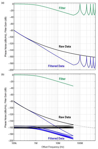
Figure 2. Illustration of phase noise in a 100 MHz input clock aliasing in a PLL by either (a) adding a PLL jitter-transfer function (green curve) to the input phase noise Raw Data (black) curve, or (b) aliasing the input phase noise located (dashed curve) above the Nyquist frequency (50 MHz) to below it (black curves) before adding it to the PLL jitter-transfer function (green curve), to derive output Filtered Data phase noise (blue) curves
As an aside, Figure 2 (b) provides an alternate view of phase noise aliasing during the sampling process [6]. Instead of mirroring the jitter-transfer function located below FS/2 across spectral boundaries located at integer multiples of FS/2 (i.e. 50 MHz) as shown in Figure 2 (a), we could alternatively fold the portion of the Raw Data curve located above FS/2 across these spectrum boundaries to appear below FS/2. Figure 2 (b) illustrates this concept, where the portion of the Raw Data curve above FS/2 (dashed curve from 50 MHz up to 500 MHz offset frequency) is aliased below FS/2. Now, the Filter curve in Figure 2 (b) can be separately added to each of the 10 Raw Data curves in Figure 2 (b) to compute the Filtered Data curves shown in Figure 2 (b). Integrating the combined area under each Filtered Data curve shown in Figure 2 (b) is mathematically equivalent to integrating the entire Filtered Data curve shown in Figure 2 (a). [7]
How Serial Data Links Observe Refclk Phase Noise
Knowing how input phase noise aliases when sampled by a PLL, we can now model the jitter-transfer function of a serial-data communications link. As an example, we'll use the common-clock timing architecture used by PCI Express [1,5], as shown in Figure 3. Here, the reference clock phase noise, X, is filtered by the transmit PLL jitter-transfer function, H1, and the receive PLL and CDR jitter-transfer functions, H2 and H3, respectively. Note that H3 is modeled for 32 GT/s links in Figure 3. The overall system jitter transfer function, Y, is a function of H1, H2, H3, and T, which is the refclk time delay between transmit and receive paths. The amount of phase noise from the reference clock that appears on the output data is therefore computed as X times Y.
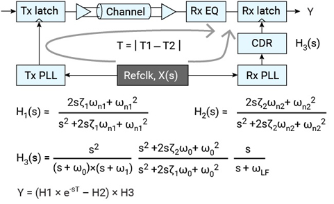
Figure 3. Illustration of PCIe5 32 GT/s system jitter-transfer function (Y) used to filter refclk phase noise (X) in a common-clock timing architecture.
PCI Express 5.0 at 32 GT/s requires filtering the refclk with 16 different system jitter transfer functions. The worst case function, which leads to the highest jitter, for a given refclk is computed and plotted between 10 kHz and 30 MHz as the green "Filter" curve in Figure 4 (a). The raw measured phase noise data is also plotted in Figure 4 (a), as a black curve labeled "Raw Data". Finally, the filtered phase noise data is computed by adding the Filter and Raw Data curves, and plotted in Figure 4 (a) as a blue curve labeled "Filtered Data."
A traditional PCI-SIG analysis evaluates TIE jitter in a 100 MHz reference clock using a real-time oscilloscope. This method samples TIE jitter at each rising edge in the clock waveform, such that spectral components of jitter above the Nyquist frequency of 50 MHz alias below 50 MHz, as done in the real system. Therefore, a TIE jitter spectrum extends up to 50 MHz, and correctly aliases higher-frequency components of jitter (as done in the real system).
By contrast, a phase noise analyzer includes a low-pass filter that prevents measuring phase noise up to an offset frequency equal to half the clock frequency (e.g. 50 MHz). It is therefore common industry practice [3] to extend the last-measured phase-noise data point up to a 50 MHz offset frequency, to match the appearance of a TIE jitter spectrum. Figure 4 (a) illustrates this practice by extending each of the three curves using red segments from 30 to 50 MHz.
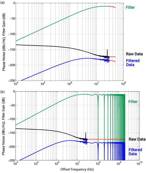
Figure 4. Example phase-noise extensions that (a) do not account, and (b) do account for phase noise aliasing when sampled by a PLL
The problem here is that a TIE jitter spectrum includes aliased components of jitter, whereas the phase noise spectrum shown in Figure 4 (a) does not. To account for aliasing, Figure 4 (b) uses (1) a red line to extend the last measured "Raw Data" phase noise data point to an arbitrary value of 2 GHz, and (2) extends the green Filter curve by mirroring it across spectral boundaries located at integer multiples of the Nyquist frequency (i.e. 50 MHz). The filtered phase noise data shown in Figure 4 (b) as a blue curve labeled "Filtered Data" now accounts for aliased components of phase noise up to an offset frequency of 2 GHz. Alternatively, as discussed above in Figure 2 (b), the phase noise could have been extended as a flat line to 2 GHz and then mirrored back to below 50 MHz before filtering (not shown). The filtered phase noise data can then be integrated to convert it to jitter. [7]
In performing this integration, we observe that the filtered phase noise below 100 kHz is sufficiently low that it can be ignored. However, the filtered phase noise around 2 GHz is significant and, in fact, dominates the integral. The result is, similar to the PLL analysis above, that we cannot define an upper-integration limit to derive jitter from the filtered phase noise. Further analysis is required.
Motivation
Our goal is to find a method to derive jitter from phase noise that matches TIE jitter traditionally measured with an oscilloscope (without jitter added from the test environment). Since an oscilloscope observes jitter similar to a real system, we regard its result as the gold standard against which other methods may be judged (assuming the oscilloscope doesn't add a significant amount of jitter, or that it can be subtracted out during post processing). The rest of this article summarizes an exhaustive study [9,10] to determine such a method [7]. The study analyzed nine different clock devices manufactured by four different companies. The devices were chosen to cover a wide range of jitter values, spanning two orders of magnitude.
Test Setups
The test setups used in this study are shown in Figure 5. The refclk jitter is measured with an oscilloscope [11] according to the traditional PCI-SIG methodology [1,5]. This study used Keysight Technologies oscilloscope model DSA91204A at 40 GS/s, whose jitter results were previously correlated with other manufactures' oscilloscopes [9]. The PCI Express 5.0 Base specification [5] requires the clock device under test (DUT) to connect directly to the oscilloscope, as shown in Figure 5 (a). Additionally, in this study, the DUT connects to either a phase noise analyzer or a spectrum analyzer instrument via an optimized [12] balun connection, as shown in Figure 5 (b). The Rohde and Schwarz (R&S) FSWP was used in both phase noise analyzer and spectrum analyzer modes. A Keysight Technologies model E5052B phase noise analyzer was additionally used to validate the final methodology.
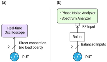
Figure 5. Test setups for measuring jitter with (a) an oscilloscope, and (b) phase noise analyzer and spectrum analyzer
Test Data
For reference, the signal integrity of each of the nine clock devices is shown in Figure 6 (a), along with a zoomed-in view of rising-edge transitions in Figure 6 (b). The clock devices are identified anonymously in the legend using letters A through I. The oscilloscope acquisition bandwidth was set to an optimum value of 2 GHz for all the devices, except device A, whose optimum bandwidth was 5 GHz. The instantaneous time crossings at 0V were interpolated and used to compute 1 million consecutive TIE jitter values for each of the 16 required GEN-5 jitter filters [5]. We'll refer to this process below as the "PCI-SIG traditional jitter method."
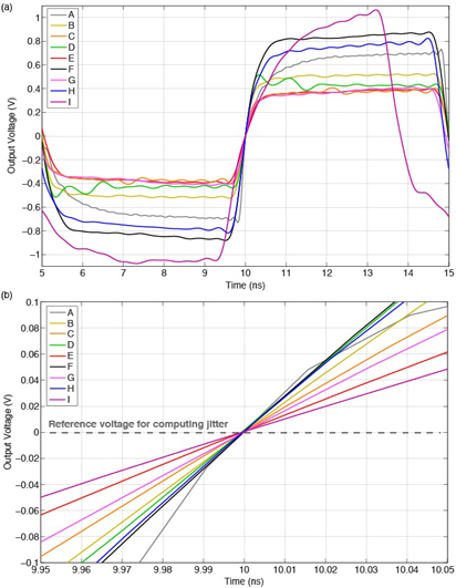
Figure 6. Acquired oscilloscope waveforms for 9 clock devices showing (a) one cycle, and (b) rising-edge transitions
Next, jitter added from the test environment was measured and subtracted [2,13] from the PCI-SIG traditional jitter values. We'll refer to this process below as the "PCI-SIG traditional jitter method minus scope vertical jitter." Of these 16 jitter values, the worst case, or highest jitter, corner is singled-out as a golden reference for comparing various phase-noise methodologies below.
The R&S FSWP instrument was initially used to analyze phase noise, with results shown in Figure 7 (a). Phase noise analyzer and spectrum analyzer modes were used below and above, respectively, 30 MHz offset frequency, marked by a vertical dashed line in Figure 7 (a). For reference, an equation for output voltage is shown at the top of Figure 7 (a) for each mode, to remind readers that a phase noise analyzer observes only phase noise (ϕ), whereas a spectrum analyzer observes amplitude noise (B), amplitude modulation (A), and phase noise (ϕ) [8]. The spectrum analyzer data extends to the device's optimum oscilloscope acquisition bandwidth. Figure 7 (b) is similar to (a), but with spurs omitted and 1% smoothing enabled. This makes it easier to observe a device's random noise floor, which rolls off, as expected, with increasing offset frequency. Figure 7 (c) plots the raw phase noise analyzer data below 30 MHz, and appends a flat extension region at higher offset frequencies up to the optimized oscilloscope acquisition bandwidth for each device.
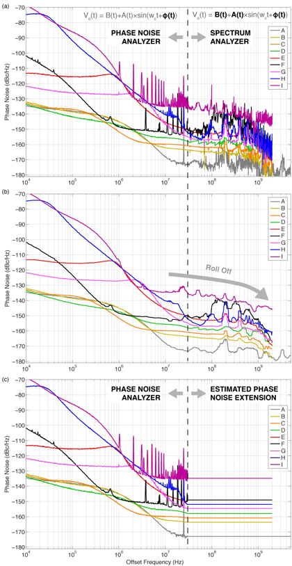
Figure 7. Measured phase noise data for 9 clock devices showing (a) raw and (b) 1% smoothed phase noise data with spurs omitted as measured by a phase noise analyzer below, and spectrum analyzer above, respectively, 30 MHz offset frequency (marked by a dashed line), and (c) raw phase-noise analyzer data only with a flat extension appended above 30 MHz
Methodology Results
Jitter is derived from Figure 7 (a) phase noise by applying the worst-case jitter filter corner observed from the oscilloscope analysis, then integrating the filtered phase noise (not shown) across all offset frequencies. We'll refer to this method below as the combined raw phase noise and spectrum analyzer method, or "combined PN + S/A method, raw." Jitter is also derived from Figure 7 (b) using the same process, which we'll refer to below as "combined PN + S/A method, smoothed." Finally, jitter is derived from Figure 7 (c) by applying the same worst-case jitter filter, then integrating the filtered phase noise data (not shown) from 10 kHz up to various offset frequencies ranging from 50 MHz to 1 GHz in steps of 50 MHz. That is, the upper integration limit is either 50 MHz, or 100 MHz, or 150 MHz, and so on, up to 1 GHz. We'll refer to this method below as the "PN to x MHz w/ flat ext." method, where x represents the upper limit for integration.
Figure 8 summarizes key jitter results. Data from the traditional PCI-SIG oscilloscope-based methodology is plotted using open-red "o" symbols. Subtracting jitter introduced by the oscilloscope's vertical subsystem from this data produces the filled-red "o" symbols plotted in Figure 8, which establish a baseline to evaluate all phase noise methodologies.
Jitter derived from the combined phase noise analyzer and spectrum analyzer modes shown in Figure 7 (a) and (b) for raw and smoothed data, respectively, are plotted in blue using triangle and "*" symbols. Note that the blue triangle for device I is at 930 fs RMS, which falls outside the plotted area. Among the jitter derived from phase-noise-with-flat-extensions shown in Figure 7 (c), the best match (to the filled-red "o" symbols) occurred for an upper integration limit of 200 MHz offset frequency. This data is plotted in Figure 8 with a green "×" symbol. For reference, the corresponding jitter for an upper integration limit of 50 MHz is plotted with a green "+" symbol. The remaining computed phase-noise-with-flat-extensions weren't noteworthy, and are omitted from Figure 8.
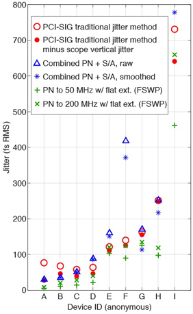
Figure 8. Summary comparing jitter results for oscilloscope and phase-noise based methodologies