
The measured impedance value shown in Figure 10 is only 0.7% less than the value calculated using ADS, as shown by Figure 5, and 0.5% less than the impedance value provided by the Rogers MWI calculator shown in Figure 6.
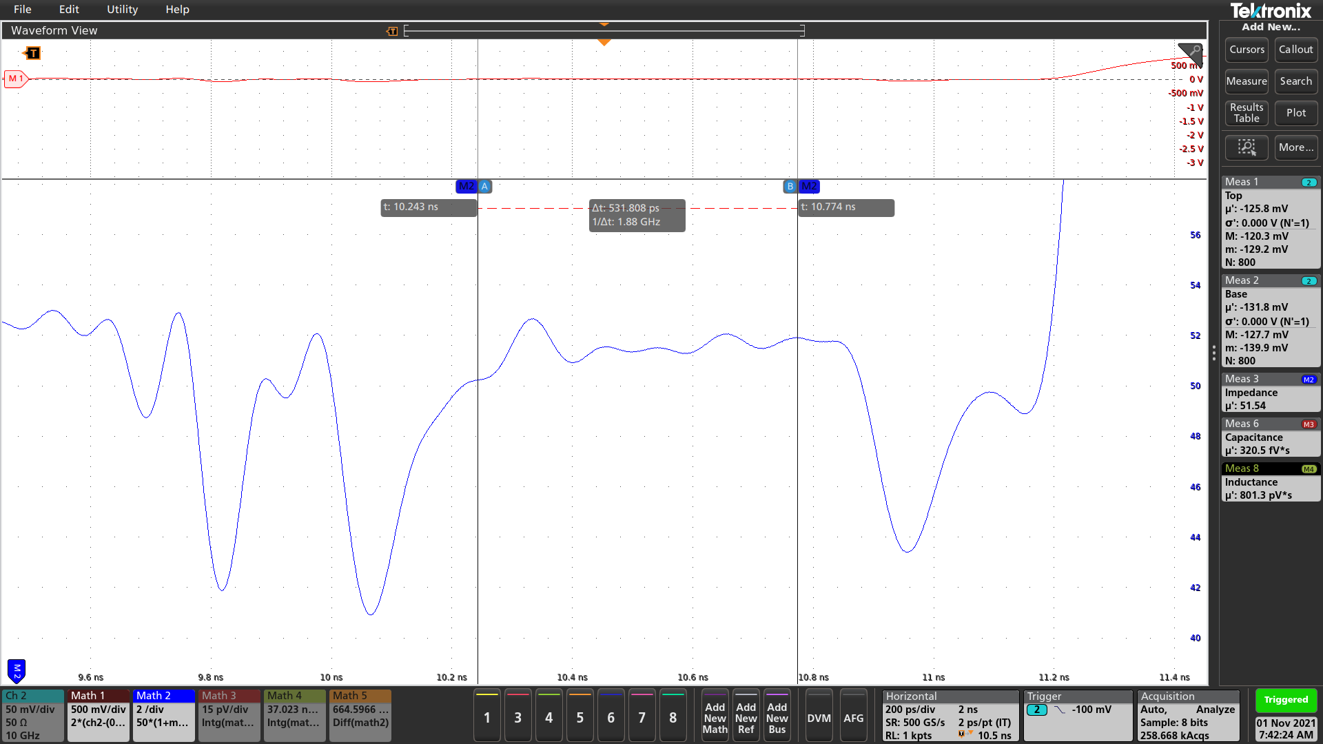
Fig. 10 - TDR impedance measurement of demo board TP5 Trace with the P2105A probe.
With reference to EQ(5), and the measured result in Figure 8 with the P2105A probe, we can calculate the demo board’s Dkeff to be:  If you recall, the Dkeff value shown by EQ(11) is within 5.1% of what we simulated using the ADS tool, and within 6.74% of the value calculated using Rogers MWI calculator. Again pointing to the fact that the specified values for bulk dielectric constants include uncertainty which varies based on copper thickness, roughness, laminate thickness variation, and PCB manufacturing tolerances. Keep in mind that simulators are ideal calculations and do not contain the same noise as a real-world measurement. The correlation between ADS and the measurement could be further improved if copper roughness was included in the ADS simulation. In addition, as previously discussed, the RO4003C laminate thickness can allow for up to a 12% variation in thickness.
Since we are measuring a microstrip, the result shown by EQ(11) is the effective dielectric constant and not the RO4003C bulk dielectric constant. This result is a combination of the bulk dielectric constant and the contribution of the field lines in air with Dk = 1, as originally shown by Figure 2. In order to compare what is actually on Rogers RO4003C datasheet for an 8 mil laminate thickness with our simulated result, we need to calculate the bulk Dk.
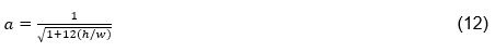
We can use a method from [10] to approximate the bulk dielectric constant, as shown in EQ(12) and EQ(13). Where EQ(12) calculates a correction factor (a), using the trace width (w) and the dielectric thickness (h).
 The demo board shown in Figures 1 and 3 has a 14.9 mil specified trace width (w) and a specified dielectric thickness (h) of 8 mils. From EQ(12), a = 0.366.
Using the correction factor, the bulk dielectric can be calculated using EQ(13):
With reference to EQ(12) as well as EQ(13) and the result shown in EQ(11), we can solve for the bulk dielectric constant Dk based on the TDR measurement as shown in EQ(14).

The bulk Dk result shown by EQ(14) is within 3.9% of the Rogers Design Dk specified value of 3.803.
The Rogers R04003C datasheet, for typical Dk value of 3.38, specifies a max Dk tolerance of 1.47% (Dk +/-0.05). Assuming this tolerance is valid towards the bulk Dk, let’s then assume our laminate is at the high end of the specified tolerance. If we compare the maximum tolerance case laminate value (3.86) to our measured value (3.95), then our result is within 2.36% of the Rogers Design Dk. The remaining error is likely due to manufacturing tolerances that occurred as a result of the slightly different pressed laminate thickness, copper roughness, and the material laminate characterization testing method.
Let’s quickly discuss why the Rogers bulk Design Dk could be reported lower than our measurement. It is very common for laminate vendors like Rogers to use a Clamped Stripline Resonator Test per IPC-TM-650 2.5.5.5 for material characterization [12]. In fact, the R04003C datasheet specifies this test method for this laminate’s characterization. However, when using this the testing method, sometimes entrapped air will cause the test to report a lower Dk.
Table 1 provides a summary of the results discussed, including the time delay per unit length (TD/inch) which can be calculated with reference to EQ(3).
As shown by Table 1, the impedances have a maximum delta of 0.5%, which occurs between our measurement and the Rogers MWI calculator. There is a 3% delta between the measured TD/inch value and the Rogers MWI TD/inch value and 0.8% delta between the simulated ADS TD/inch value and the Rogers MWI TD/inch value. However, since the ADS simulation is based on the same Rogers Design Dk value as an input, it would be expected that these agree with each other.
Table 1 - Summary of Rogers RO4003C Dkeff Design Dk, Simulated, and Measured Values
|
Dkeff |
Delta Dkeff from Rogers MWI Result |
Impedance (Ω) |
Delta Impedance from Rogers MWI Result |
TD/inch |
Delta from Rogers MWI TD/inch Result |
Rogers MWI Simulated Value |
2.8255 |
N/A |
51.80 |
N/A |
141.73 ps/in |
N/A |
ADS Simulated Value |
2.869 |
1.54% |
51.91 |
0.21% |
142.82 ps/in |
0.8% |
TDR Measured Value |
3.016 |
6.74% |
51.54 |
0.5% |
146.43 ps/in |
3% |
As a final effort to understand what could be causing the majority of the error between our measurement and the Rogers Design Dk, we used the measured bulk Dk = 3.95 as an input into the ADS simulator. With reference to Figure 11, by varying the RO4003C laminate thickness, we found at the minimum RO4003C laminate thickness (7 mil) allowed within the vendor’s specified tolerance, that the ADS simulation was able to provide a Dkeff = 3.00063, which is within 0.5% of our measured Dkeff = 3.016. As we discussed previously, unfortunately, from the reported PCB cross section we did not know for sure the actual manufactured RO4003C laminate thickness.

Fig. 11 - Keysight PathWave ADS Controlled Impedance Line Designer with 7 mil thickness material laminate and measured bulk Dk.
Lastly, we had a sample of the 50 TDR demo boards tested by the fabricator. With reference to Figure 12, the first row is trace 1 impedance, measured on 5 of the 50 demo boards. The second row is the measurement of the differential coplanar traces, which are 50Ω single ended and 100Ω differential. Interestingly, the spread of the five, 50Ω measurements, is +/-4.86% and the spread of the differential trace is 2.8%. The trace isn’t particularly narrow at 15 mils, so we suspect this is mostly the tolerance of the material. It is just one double sided laminate. The smaller variation of the differential traces suggests that this is random tolerance. Two side by side 50Ω traces, if they have random tolerances would be a factor of square root of two better than a single trace, as this seems to indicate.
Of course this test data is a random sampling of one trace on five of the 50 produced boards. We measured one of the 50 random boards for this article, so extrapolating the expected tolerance using double sided standard deviation, the 4.9% seems quite reasonable, and likely largely dominated by the laminate.
All of this further emphasizes the point of the laminate’s datasheet uncertainty and the importance of using a measurement to further improve the fidelity in your design.
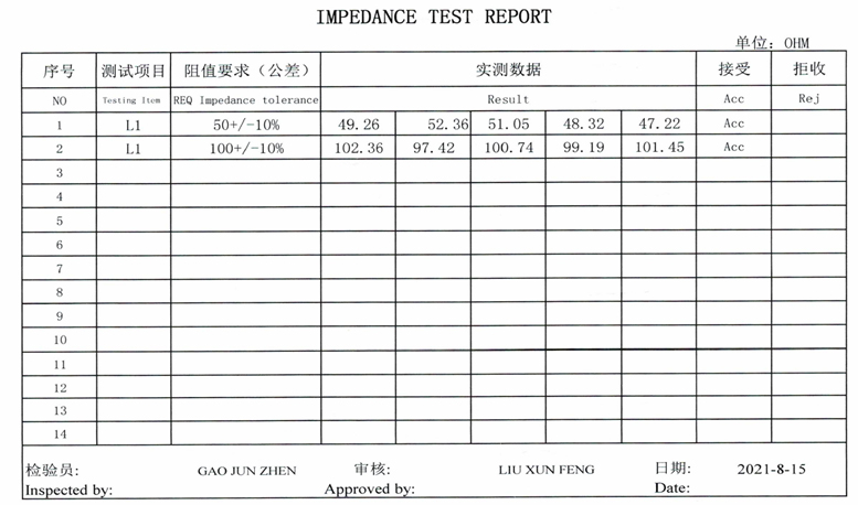
Fig. 12 - PCB Fabricator Impedance Test Report for 5 Picotest TDR demo boards.
To wrap up our analysis, it is important to note that the TDR demo board does not use a solder mask. The results will be further impacted when a solder mask is applied over the microstrip, since field lines will pass through the dielectric, air, and the solder mask. In addition, solder mask increases dielectric loss.
Conclusion
As discussed earlier, since the trace measured on the TDR demo board is a microstrip, the results shown by EQ(11) do not represent the bulk dielectric constant. However, the result shown by EQ(14) does represent an approximated value for the bulk dielectric constant, which is shown to be within a reasonable tolerance to the datasheet value for Rogers RO4003C. As shown in this article, we can convert the measured effective dielectric constant into the bulk laminate dielectric constant. This method was also confirmed using a 2D field solver. These methods demonstrated good correlation from simulation to measurement for impedance of a transmission line. Despite the good correlation, we have shown that there are many tolerances that impact the results, and that a five sample measurement resulted in a 4.9% tolerance. A double-sided interval with reasonable confidence would be much larger. This further emphasizes the importance of verifying these results with a measurement such as a TDR and explains the significant cost increase for tighter tolerance impedance control.
References
- Application Note - TDR Measurement using J2154A and MSO68B Oscilloscope
- Pozar, D. M. (2012). Microwave engineering / David M. Pozar, University of Massachusetts at Amherst (4th ed.). Wiley.
- Practical Measurements of Dielectric Constant and Loss for PCB Materials at High Frequency
- Rogers RO4003 Series High Frequency Circuit Material Site
- Rogers Corp RO4000 Series High Frequency Circuit Materials
- Keysight Pathwave ADS
- Rogers MWI Calculator
- Design Right the First Time: Understanding how Dielectric Constant (Dk) Test Methods Affect Time to Market
- IPC-TM-650 Test Methods Manual 2.5.5.7 Characteristic Impedance of Lines on Printed Boards by TDR
- Bogatin, E. Bogatin’s Practical Guide to Transmission Line Design and Characterization for Signal Integrity Applications. Artech House, 2020.
- Tektronix 6 Series B Mixed Signal Oscilloscopes Specifications and Performance Verification (MSO64B, MSO66B, MSO68B)
- IPC-TM-650 Test Methods Manual - 2.5.5.5 Stripline Test for Permittivity and Loss Tangent
- Picotest J2154A PerfectPulse® Differential TDR
- Picotest P2105A - 1 Port PDN Transmission Line Probe
- Tektronix MSO68B Oscilloscope
- Picotest PDN Cable
- S. Sandler. “Simple trick to measure plane impedance with a VNA.” EDN
- Bogatin, E. et al. “Quick and Easy Dielectric Constant Measurements.” Signal Integrity Journal, May 2020.