
When doing printed circuit board (PCB) stackup and signal integrity (SI) impedance modeling, we need to get the dielectric material properties from the right sources. One important parameter for accurate impedance modeling is relative permittivity (εr) of the dielectric material, otherwise known as dielectric constant (Dk). The best source is from laminate suppliers’ data sheets. Though there is an issue with these I like to think of as, “a tale of two data sheets.”
Marketing data sheets, like the example shown in Figure 1 [6], are easily found on laminate suppliers’ websites. They are meant for quick comparison of dielectric properties to narrow your search for the right laminate for your application. Dielectric properties on marketing data sheets include mostly thermal and mechanical properties, which are important for the physical structure of the material and how it will perform with other material properties in the stackup during processing.
But marketing data sheets are not representative of what is needed to design an actual stackup, or to do impedance and SI loss modeling. Depending on glass style, resin content, thickness, Dk, and dissipation factor (Df) will be different for different cores and prepreg thicknesses for the same laminate. Marketing data sheets usually only report a typical Dk/Df at fifty percent resin content and two or three frequency points. Thickness is not specified. Furthermore, Dk and Df are not constant over frequency. So, using numbers from these data sheets will lead to inaccurate impedance and phase delay results.
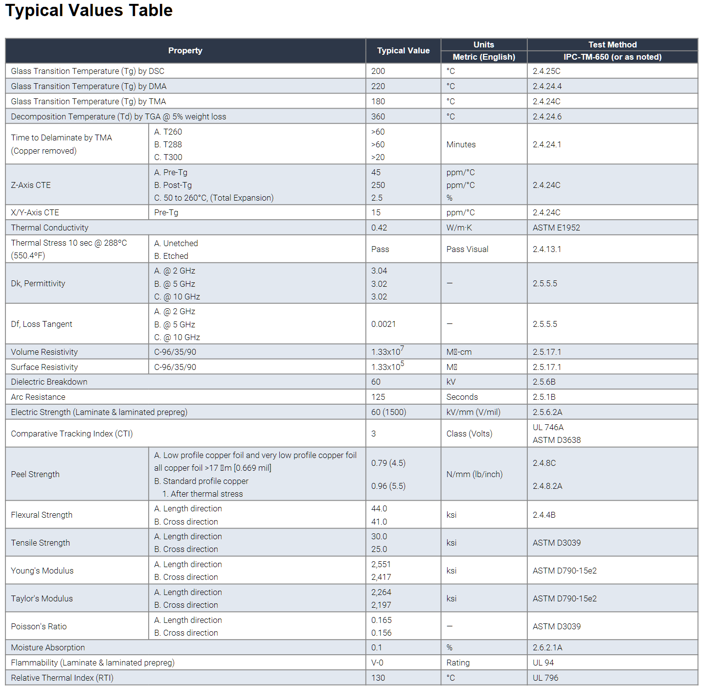
Figure 1. Example of a “Marketing” data sheet easily obtained from laminate supplier’s web site. Source Isola Group [6].
Instead, for transmission line modeling, one needs to use the same Dk/Df table data sheets PCB fabricators use to build the stackup. An example Dk/Df table is shown in Figure 2. Dk/Df tables provide the actual core and prepreg thicknesses, resin content, and Dk/Df for the different glass styles, over different frequencies. Depending on the stackup, a combination of thicknesses is often needed to meet impedance requirements. Each thickness will have a different Dk value.
In the example of Figure 2, Dk varies from 2.92 at 10 GHz for 1080 glass style to 3.19 at 10 GHz for 2116 glass style. This represents a Dk variation of -3.3% to 5.6% when compared to a Dk of 3.02 at 10 GHz specified in Figure 1.
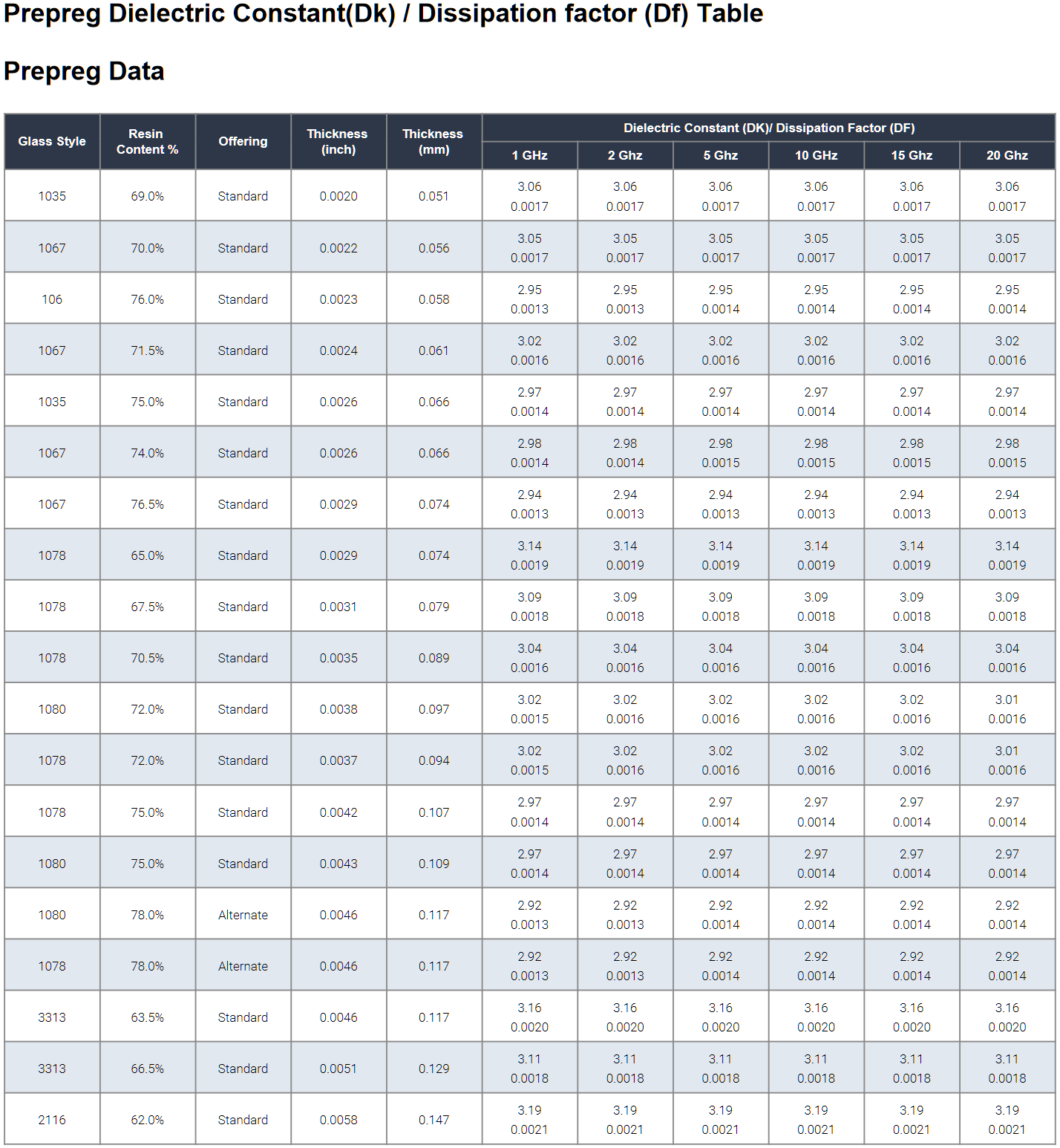
Figure 2. Example of a typical “Engineering” data sheet showing Dk/Df table for different glass styles and resin content over frequency. Source Isola Group [6].
Many engineers assume Dk published is the intrinsic property of the material. But, in fact, it is the effective Dk (Dkeff) measured by a specific industry standard test method. When they are compared against real measurements from a design application, there is often a discrepancy in Dkeff due to increased phase delay caused by surface roughness [1].
Dkeff is highly dependent on the test apparatus and conditions of how it is measured. One method commonly used by many laminate suppliers is the clamped stripline resonator test method, as described by IPC-TM-650 2.5.5.5, Rev C, Test Methods Manual [10].
Since all glass reinforced laminates are anisotropic, any stripline based test method, like TM-650 2.5.5.5, or Bereskin stripline test method [13], reports Dk values in which the E-fields are transverse to signal propagation. That is, if the signal propagation is in the x-y axis direction, then the Dk measured by this method is when E-fields are in the z-axis direction.
For Isola’s Dk/Df table [6], shown in Figure 2, Dk values were measured by TM-650 2.5.5.5 test method. From that data, the values for most of the constructions are calculated. Additional verification runs are performed to gather statistical data over time and validate that the calculations are reasonable and accurate.
The measurements are done under stripline conditions using a carefully designed resonant element pattern card. It is made with the same dielectric material to be tested. As shown in Figure 3, the card is sandwiched between two sheets of uncladded dielectric material under test. Then the whole structure is clamped between two large plates; each lined with copper foil and grounded. They act as reference planes for the stripline.
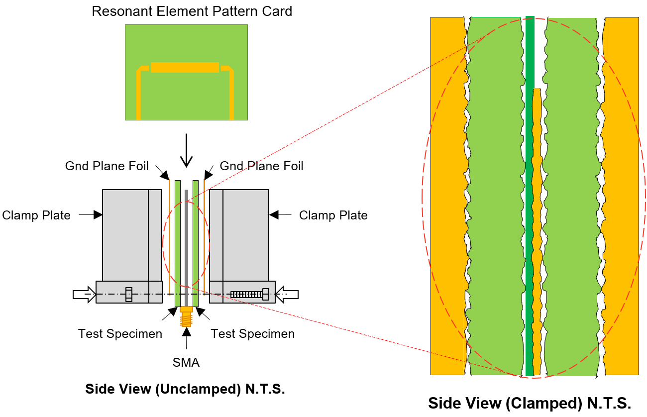
Figure 3. Illustration of clamped stripline resonator test method, as described by IPC-TM-650, 2.5.5.5, Rev C, Test Methods Manual [10].
This test method assures consistency of product when used in fabricated boards. It does not guarantee the values directly correspond to design applications.
Here is why:
Since the resonant element pattern card and material under test are not physically bonded together, air is entrapped between the various layers. These small air gaps are caused by the:
- roughness of the copper foil plates in the fixture
- roughness profile imprint left on the surface from the foil that was removed from the test samples
- copper removed on the resonant element pattern card
Air entrapment, due to the TM-650 test method, is the primary reason for effective Dk and phase delay discrepancies between simulation using laminate suppliers’ Dk/Df tables and real measurements from a design application. The small air gaps result in a lower effective Dk than what would be measured in a real PCB because everything is pressed together with no air entrapment, as shown in a cross-section view of Figure 4.
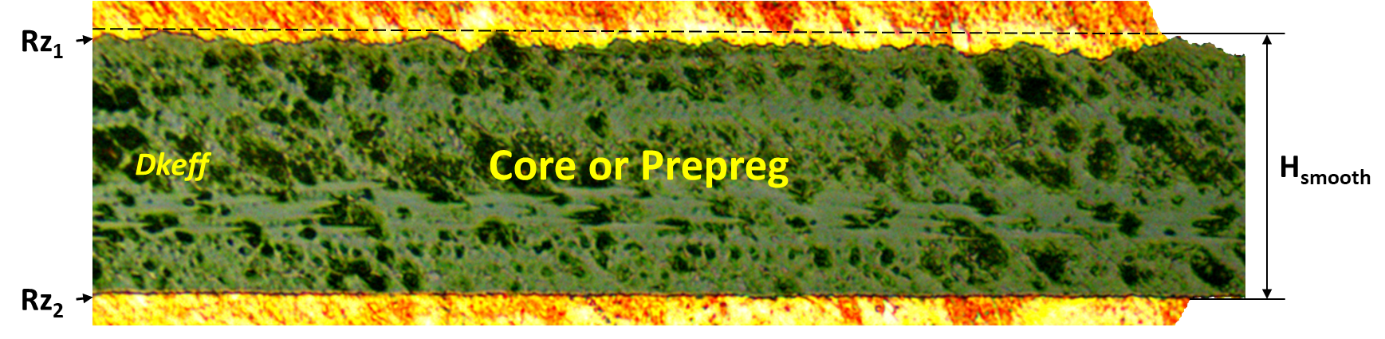
Figure 4. Example of foil bonded to core or prepreg dielectric. Rz1 is rougher than Rz2 and Hsmooth is the thickness of the dielectric as if the foil was removed.
When copper roughness is different on each side of the dielectric, like the example shown in Figure 4, Dkeff is determined heuristically by this simple correction factor:
Equation 1. 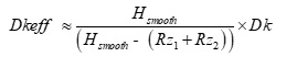
where:
- Hsmooth is dielectric core thickness from laminate suppliers’ Dk/Df table data sheet or pressed prepreg thickness from the PCB stackup drawing.
- Rz1 and Rz2 are the conductor roughness of the foil for the respective side of the dielectric from foil suppliers’ data sheet. Typically, Rz is the 10-point mean roughness as measured by a mechanical profilometer.
- Dk is dielectric constant from laminate supplier’s Dk/Df table data sheet.
In Figure 4, Rz1 is the roughness of the top foil, and Rz2 is the roughness of the bottom foil. In this example, Rz1 is rougher than Rz2. Hsmooth is the core thickness of the dielectric, as specified in the Dk/Df table, or pressed thickness of the prepreg, often shown on a stackup drawing. It is the thickness of the dielectric as if the foil was removed.
When copper foil with the same Rz roughness is bonded to each side of the core or prepeg, Dkeff can be simplified as:
Equation 2. 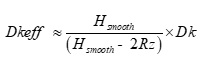
Figure 5 plots Dkeff over frequency derived from S21 phase or time delay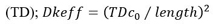 from a Megtron-6 stripline case study [3]. This method is different than IPC-TM-650 test method in that it determines Dkeff from unwrapped phase delay rather than calculating Dk/Df from resonant peaks over the frequency range defined in the spec.
The blue plot is a simulated case based on core and prepreg Dk values from published Dk/Df tables at 12 GHz. When Dk is corrected due to roughness, using Equation 2, and resimulated, Dkeff is shown in pink. Although the Dkeff has improved, it still does not agree with the measured Dkeff from the device under test (DUT), shown in red.
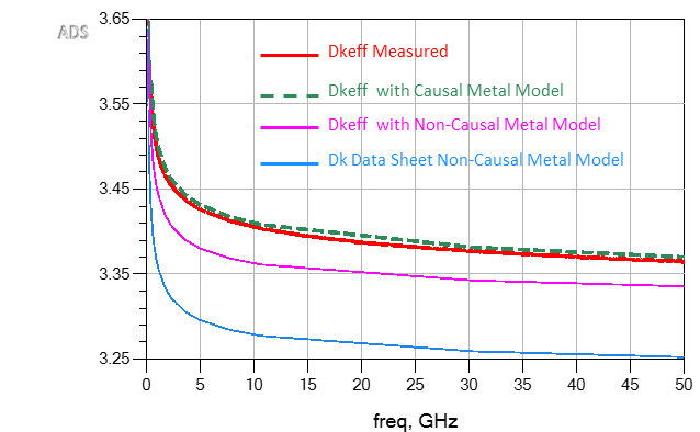
Figure 5. Comparisons of simulated Dkeff over frequency vs. measured. The red plot is actual measured Dkeff from the DUT. The middle pink plot is a simulation using Dkeff corrected due to roughness. The bottom blue plot is simulated using Dk at 12 GHz as published in Dk/Df tables and non-causal roughness model. The green dashed plot is a simulation using Dkeff due to roughness; a causal Huray-Bracken roughness model was used. Modeled with Simbeor [11] and simulated with Keysight ADS [12].
The discrepancy between the pink and red plots is because Dkeff from Equation 2 only corrects the phase delay due to self capacitance (C11) per unit length of the transmission line. But roughness of the foil also increases the self inductance (L11) per unit length of the transmission line, which adds additional phase or time delay [4].
This is counter intuitive and can be confusing since we usually relate Dkeff to capacitance only. By definition, Dkeff is the ratio of the actual structure's capacitance to the capacitance when the dielectric is replaced by air. But this is only true for static electric fields. For time-variant electromagnetic fields, Dkeff becomes frequency-dependent [14].
If the propagation delay (tpd) for a single transmission line, in seconds per unit length, is determined by:
Equation 3. 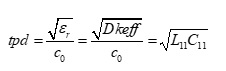
and c0 is the speed of light is permeability and permittivity of free space respectively, then:
Equation 4. 
where: L11; C11 are self inductance in Henries per unit length and self capacitance in Farads per unit length respectively.
Equation 4 clearly shows that with an increase in self inductance there will be a proportional increase in Dkeff. This means for PCB transmission lines, calculating cannot be trusted to be the same as relative permittivity (εr) of the dielectric material. The consequence for doing so leads to inaccurate impedance predictions and non-causal time domain simulations, resulting in poor correlation to measurements.
A causal model, when simulated, does not produce any change in its output signal before there is a change in its input signal. When field solvers properly correct the self inductance, by applying the roughness correction factor to the imaginary portion of the complex impedance of the metal [4][5], the model is then causal. When combined with the corrected Dkeff for cores and prepregs from Equation 2, there is excellent correlation, as shown by the dashed green plot in Figure 5. Unfortunately, not all field solvers have causal roughness models to correct the inductance in the simulation.
Since there is no simple way to backtrack from a phase measurement to establish the right Dkeff to use for your modeling, especially for lossy stripline constructions, heuristic methods are an alternative.
Using the right Dkeff for your modeling ensures a correct time domain reflectometer (TDR) impedance prediction, as shown in Figure 6. The red plot is measured differential TDR from [3]. When core and prepreg Dk from Dk/Df tables were used along with a non-causal roughness model in the simulation, the blue plot shows an overestimate for impedance. When Dkeff from Equation 2, and a non-causal roughness model was used in the simulation, the pink plot shows an underestimate in the impedance plot.
It is only when we apply a causal Huray-Bracken roughness model from [11], along with Dkeff from Equation 2, that we see the effect of the increased self inductance, shown by the green dashed line plot in Figure 6.
At first glance of Figure 6, one might interpret the pink plot as having better correlation to the measured red plot. But because the measured plot has an impedance ripple along its length, it is difficult to conclude which is the correct model from the TDR plots alone. It is only when we compare Dkeff derived from the green dashed phase delay plot from Figure 5 that we can conclude the green dashed line TDR plot is the correct impedance.
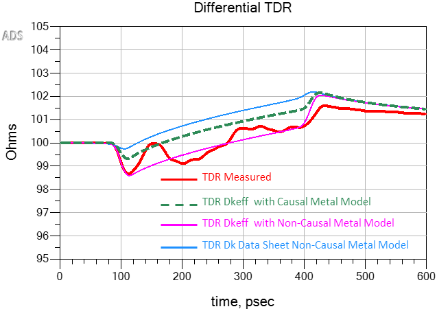
Figure 6. Simulated vs. measured differential TDR plots when different Dkeff was used in the model. The blue plot overestimates impedance when Dk from data sheets was used. The pink plot underestimates the impedance when Dkeff (Equation 2) and non-causal roughness model was used. The green dashed line plot is when Dkeff (Equation 2) and a causal Huray-Bracken roughness model were used. Modeled with Simbeor [11] and simulated with Keysight ADS [12].
Summary:
Dielectric constants from marketing data sheets cannot be trusted to properly design PCB stackups and model transmission lines for impedance and phase delay. Instead, laminate suppliers’ Dk/Df tables should be used.
Many laminate suppliers provide Dk/Df tables derived from a clamped stripline resonator test method [10] or similar Bereskin test method [13]. But the numbers do not factor the actual roughness of the foil. When a simple correction factor, based on the thickness of laminate and Rz foil roughness is considered, a more accurate value for Dkeff along with a causal roughness model can be used for impedance and transmission line modeling.
For PCB transmission lines, calculating Dkeff from phase or time delay measurement method cannot be trusted to be the relative permittivity of the dielectric material. Using this value will lead to inaccurate simulation results.
References:
- L. Simonovich, "A Practical Method to Model Effective Permittivity and Phase Delay Due to Conductor Surface Roughness", DesignCon 2017, Santa Clara, USA.
- B. Simonovich, “Stackup Beware: Case Study of the Effects on Transmission Line Losses Due to Mixed Reference Plane Roughness”, Signal Integrity Journal article, August 10, 2021.
- B. Simonovich, “PCB Fabrication: What SI/PI Engineers Need to Know for First Time Modeling Success”, DesignCon 2021 Spring Break Webinar Series, April 12-16, 2021.
- V. Dmitriev-Zdorov, B. Simonovich, Igor Kochikov, "A Causal Conductor Roughness Model and its Effect on Transmission Line Characteristics", DesignCon 2018, Santa Clara, USA.
- J.E. Bracken, “A Causal Huray Model for Surface Roughness”, DesignCon 2012, Santa Clara, USA.
- Isola Group, 6565 West Frye, Chandler, AZ 85226.
- Circuit Foil, 6 Salzbaach, 9559 Wiltz, Grand Duchy of Luxembourg.
- Rogers Corporation, 2225 W. Chandler Blvd., Chandler, AZ 85224.
- J. Coonrod, “Managing PCB Materials: Dielectric Constant (Dk)”, Rogers Corporation, Blog Article, Sep 11, 2018
- IPC-TM-650, 2.5.5.5, Rev C, Test Methods Manual
- Simbeor THz [computer software].
- Keysight ADS Keysight Advanced Design System (ADS) [computer software].
- Bereskin, A. B. “Microwave Dielectric Property Measurements”, Microwave Journal, vol. 35, no.7, pp. 98 – 112
- Wikipedia contributors. (2022, January 12). Relative permittivity. In Wikipedia, The Free Encyclopedia. Retrieved 18:14, January 14, 2022.