
It’s what you don’t know you don’t know that can ruin your day. This paper notes in detailed examples that with today’s high-speed designs, we can no longer restrict our thinking in terms of signal integrity, power integrity or EMC alone. We must consider all three disciplines and become educated about each of them to achieve successful designs.
When discussing signal integrity (SI) issues there is always a great debate when signals on one layer of a printed circuit board (PCB) crossing over split or a slot in the reference planes on an adjacent layer. On the one hand, some argue that crossing a split plane should never be done because of the increased risk in crosstalk and possible failure to pass electromagnetic compatibility (EMC) compliance. On the other hand, others stressed that if the width of the gap and power/ground layers in the stackup were engineered carefully, this may not be as big of an issue. So who’s right?
Well, like all things involving signal integrity, the answer is, “it depends.” And the best way to answer “it depends” is to put in the numbers. This paper attempts to dispel some of the myths about signals crossing split planes.
To start off with let us look at a typical 4 layer PCB ~ 62 mils thick with a stackup shown in Figure 1. The outer two layers are microstrip signal layers and the inner two layers are power and ground. The trace widths are 7 mils wide with 8 mil separation. When driven differentially the impedance is ~100 ohms; and when driven signal-ended (SE), the impedance is ~ 56 ohms.
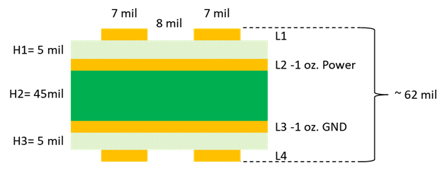
Figure 1 Simple 4 layer PCB stackup
It is common nowadays to have multiple power rails in modern designs. On a 4-layer board this means the power layer, more often than not, will be split up, and, as a result, traces crossing splits or slots on adjacent reference planes are often unavoidable.
Let’s assume we have a pair of traces on the top layer crossing a 50 mil gap on the adjacent layer as shown in Figure 2. The cross-section of the microstrip sections before and after the gap sees the dielectric thickness (H1) from the top layer to the power reference plane. Because the gap section has no reference plane on the adjacent power layer, the next reference plane is the GND layer adjacent to the bottom layer. As a result, the dielectric thickness across the gap equals the thickness of H1 plus the thickness of the 1 oz. power layer (t2) plus the thickness of the next dielectric layer (H2). If the thickness of the 1 oz. power layer is 1.2 mils, then the total thickness of dielectric is 51.2 mils across the gap.
A first order approximation of this topology is a combination of three transmission line segments with two different impedances. The first and last segments are 100 ohms differential and 56 ohms SE, while the trace impedances across the gap are ~134 ohms differential and ~103 ohms SE. Since the impedance across the gap is higher than the first and last segments, we expect to see be a positive reflection over the length of the gap. The height and width of the reflection will be a function of the rise-time and geometry of the gap. A fast rise-time with a long gap will give a higher reflection than a slow rise-time and a short gap.
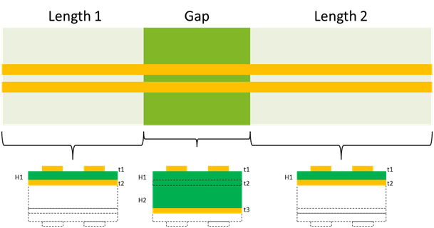
Figure 2 Cross-sectional geometries relative to gap model topology
To see just how much of an issue this is we can quickly model and simulate it with Keysight ADS [1] as shown in Figure 3. Two transmission line segments before and after the gap section were modeled with internal 2D field solver using the “TLines-Line Type” pallet. The gap section was modeled and simulated with Momentum 3D planar field solver in order to properly capture the electromagnetic effects as the signals cross the gaps. Both shared the same substrate definition. The S-parameter results from Momentum were saved in touchstone format and brought back into the ADS schematic.
The total length of the topology is 2.650 inches. The first section, Length 1, is 500 mils and the last section, Length 2, is 2 inches. The 3D model sections is broken up into three 50 mil sections to facilitate gap adjustment and ensures total length remains the same.
Two gap lengths are chosen to compare a small vs large gap. It is not uncommon to have 50 mils separation between power planes, so that is what was used for worst case gap. A 5 mil gap is chosen for best case, which is a typical minimum for trace to pad clearance spec.
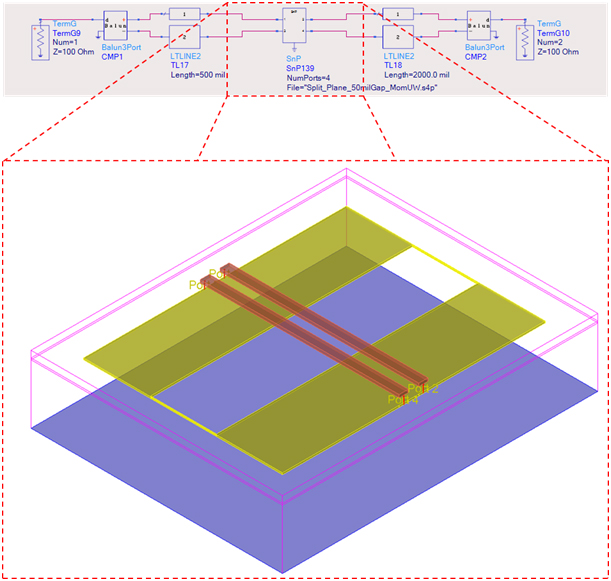
Figure 3 Keysight ADS general schematic used to model and simulate a microstrip split plane
When the topology is driven differentially from Port 1, the comparison for differential impedance is shown in Figure 4. Balun transformers are used to convert from 4-port to 2 port for convenience. As expected, for the 50 mil gap shown in red, there is a higher impedance discontinuity than the 5 mil gap, shown in blue.
This is because the height of the reflected pulse is determined by a combination of the spatial length of the rise-time and the gap width. Since the spatial length of the rise-time is less than the gap width, it never reaches the full magnitude of the impedance discontinuity.
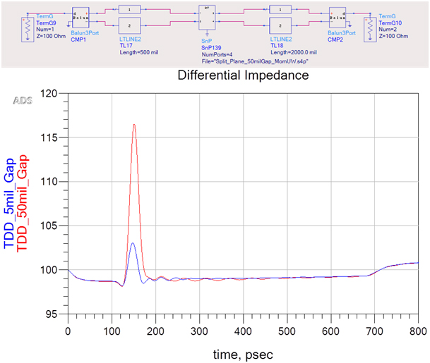
Figure 4 Differential impedance comparison of 50 mil gap (red) vs 5 mil gap (blue)
To prove it, we can drive the 50 mil gap topology from Port 2 and compare it to port 1, as shown in Figure 5. Since the edge has to propagate 2.05 inches before reaching the gap, it is slower because of dispersion caused by the lossy transmission line. Sure enough the magnitude of the reflection is lower, as we predicted.
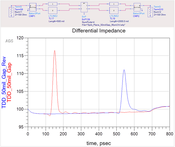
Figure 5 Differential impedance of topology with 50 mil gap when driven from each end. The slower rise-time caused by dispersion results in less reflection after 2.05 inches (blue) compared to higher reflection after 550 mils (red).
Next, single-ended (SE) transient analysis was done and results are shown in Figure 6. Red plots are with a 50 mil gap. Blue plots are with a 5 mil gap. Black plots are with no gap. The incident signal, with a risetime of 20 ps, shows the reflected voltages at the respective gaps compared to no gap. As expected it is highest for the 50mil gap. The transmitted signal shows increased risetime degradation for the 50 mil gap causing a slight increase in transmission delay.
The plot also shows the classic near-end crosstalk (NEXT) and far-end crosstalk (FEXT) signatures for all three cases. The higher incident reflections manifest themselves into higher NEXT due to the close coupling of the traces crossing the gap.
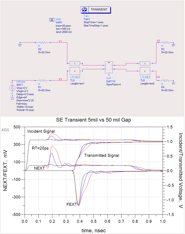
Figure 6 Comparison of single-ended Incident/Transmitted signals, NEXT/FEXT for 5 mil gap (blue plots); 50 mil gap (red plots); and no gap (black plots). The higher incident reflections manifest themselves into higher NEXT due to the close coupling of the traces crossing the gap, but there is very little increase in FEXT magnitude for either case.
Although there is a significant increase in the NEXT pulse across the 50 mil gap, there is very little increase in FEXT magnitude for either case compared to no gap. Unlike the NEXT voltage, the peak value of FEXT voltage scales with the coupled length. It peaks when its amplitude grows to a level comparable to the voltage at 50% of the aggressor’s risetime at a certain time delay (TD).
In the same way the aggressor waveform couples FEXT voltage onto the victim, FEXT couples noise back onto the aggressor affecting the risetime as shown. Due to superposition, the aggressor waveform at the far end is the sum of the FEXT voltage and the original transmitted waveform that would have appeared at TD with no coupling. Because the far end is 2.65 inches away, the FEXT is approaching saturation.
If we reduce the last transmission line segment (TL45) to 100 mils then probe before and after the gap section (SnP11), as shown in Figure 7, we can better understand the effect the gap has on FEXT.
The red plot is the incident signal (V7), with a risetime of 20 ps. The cyan plot is the transmitted signal (V8) at the far end. The light blue plot is NEXT at V5, and the light green plot is FEXT (V6) at the far end. The dark blue plot (V15) is the transmitted signal after TL44 and is the aggressor signal for V13 node. Because the gap section has a higher characteristic impedance across the gap, we observe an overshoot caused by the increased reflection for the length of the gap.
The orange plot (V13) shows the negative FEXT pulse, coinciding with the rising edge of the aggressor at V15. It also shows the increased NEXT pulse coinciding with the positive reflection on V15. As the aggressor signal propagates through the gap section, the additional voltage swing of the reflection increases the magnitude of the FEXT pulse, and the inverted shape mirrors the reflected pulse shape, as shown by the dark green plot (V14). The FEXT pulse then couples back onto the aggressor signal and degrades the risetime by the time it leaves the coupled section, as shown by the magenta plot (V16).
After the aggressor signal propagates through the last transmission line segment (TL45), the FEXT pulse increases in magnitude proportional to the length. In this case it hasn’t maximized because the last segment is only 100 mils.
The takeaway message is that when signals cross a split plane, the transmitted signal sees an impedance mismatch causing a positive reflection for a time equal to the length of the gab, which increases the magnitude and shape of the FEXT pulse, thereby degrading the risetime of the transmitted signal proportional to the FEXT pulse shape.
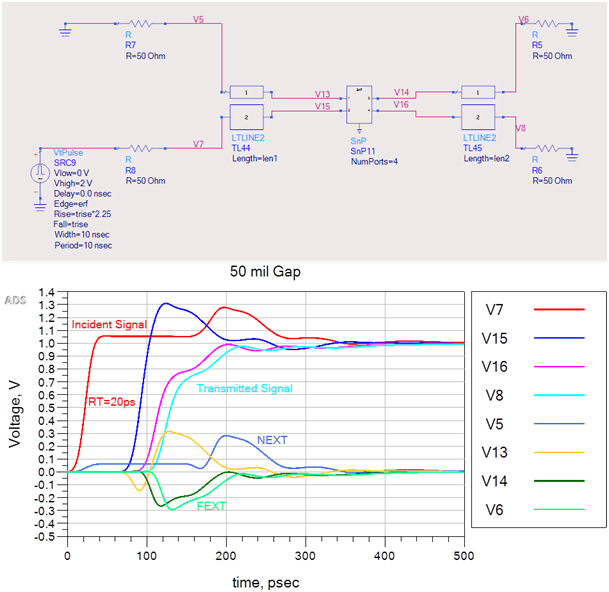
Figure 7 Single-ended transient response showing NEXT/FEXT and transmitted signals at various node points.
The combination of the split plane and diverted return current along the split edge creates an efficient slot antenna which will radiate noise. To meet FCC class B radiated emissions at 3 meters; radiated noise has to be less than 100 microvolts/m from 30-88 MHz and less than 200 microvolts/m between 216 MHz – 1 GHz. At these low voltage levels it doesn’t take much current to fail EMC.
Because the return current of traces in a microstrip geometry is discontinuous when it crosses a split plane, any noise generated will radiate into free space because there is no shielding layer above the trace to contain it. We can visualize return current behavior on the adjacent reference plane as it crosses the split using Momentum 3D viewer.
Figure 8 compares how SE return current density behaves on the reference planes when a 4 GHz sine wave signal crosses a 50 mil gap on the left and a 5 mil gap on the right. This frequency was chosen because it is the Nyquist frequency of an 8 GT/s PCIe Gen 3 link we might find on a typical 4 layer PCIe board. When one trace is driven from port 1 to port 2 while port 3 and port 4 are terminated, we can clearly see how the return current density on the reference plane behaves at the split.
We note the slight increase in current density along the edge of the victim trace across the split. This suggests that some of the current returns on the adjacent trace which accounts for the additional NEXT pulse discussed earlier. From this picture alone it is probably not a good idea to cross a split plane with single-ended driven traces.
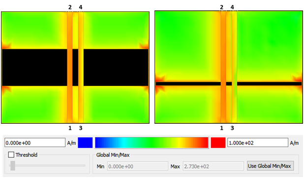
Figure 8 Example of how return current density behaves on the reference planes as a 4GHz SE signal crosses a 50 mil gap (left) and 5 mil gap (right).
Figure 9 compares how differential return current density behaves on the reference planes when a 4 GHz signal crosses a 50 mil gap on the left and a 5 mil gap on the right. As we can see, the maximum current density concentrates at the plane split edges between the differential pairs, with a small amount spreading out along the split.
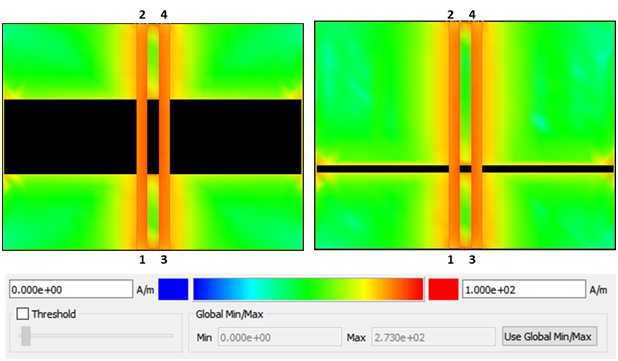
Figure 9 Example of how return current density behaves on the reference planes as a 4GHz differential sine wave crosses a 50 mil gap (left) and 5 mil gap (right).
Figure 10 shows the direction of current flow on plane layers L2 and L3 when the trace connected to ports 1-2 is driven single-ended, while the other trace is terminated. We observe that when the current direction is from port 2 to port 1 on the trace, the return current on L2 splits left and right when it reaches the far side (port 1 side) of the gap. It then goes around the gap and meets back up under the trace and returns to port 2.
We also observe there are two counter rotating current flows on L3. They are approximately centered on the left and right halves of the gap. They are caused by the injection of EM energy into to the plane cavity, due to counter rotating current along the gap edges on L2. We note the direction of current rotation is opposite on L2 compared to L3.
But when the two traces are driven differentially, as shown in Figure 11, we see that current flow along each half of the gap is in the same direction. We also note that rotation of current is in one direction on L3, centered between the differential pair and in the middle of the gap.
The takeaway message is that even when two traces are driven differentially, there is still current flow along the gap edges which will inject noise into the cavity as well as radiate into free space, resulting in EMI.
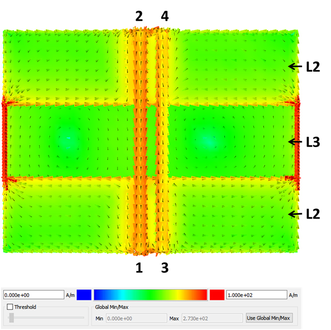
Figure 10 Return current flow on reference planes L2 and L3 when trace connected from port 1 to port 2 is driven single-ended while the other trace is terminated at each end.
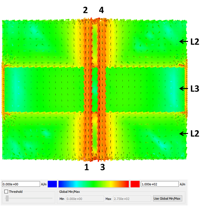
Figure 11 Return current flow on reference planes L2 and L3 when both traces are driven differentially.
So far the differential pair scenarios we have analyzed assume a perfect intra-pair skew match. But in real life this rarely happens. Issues like routing length mismatch, fiber weave effect, connector pin length differences, or asymmetrical placement of return vias, when differential traces change layers, will cause intra-pair skew. When this happens, some of the differential signal gets converted to common signal as illustrated in Figure 12. The amount is relative to how much intra-pair skew there is.
In a perfectly balanced differential pair, Vdiff is the difference of voltage between the P/N signals. If they are exactly 180 degrees out of phase, the resulting differential voltage is double and there is no common voltage.
The moment there is skew; they are no longer 180 degrees out of phase. When the difference is taken, the differential signal distorts and a common voltage (Vcom) is generated. The magnitude and shape of Vcom is proportional to the amount of phase shift. When P and N are exactly in phase with one another, there is 0% differential voltage and 100 % common voltage.
The resulting common voltage needs a current return path as well and if it is interrupted, its return current behaves like a single-ended return current crossing a split plane.
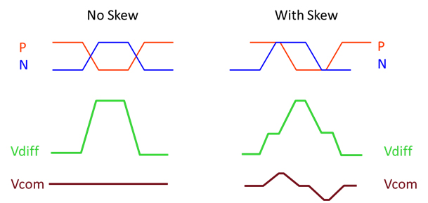
Figure 12 Differential to common signal conversion due to P/N phase shift known as skew.
The PCIe External Cabling Specification, Revision 1.0 [2] worst case skew budget is 21% of a unit interval (U.I.), where one U.I. is equal to the bit time. Using 0.21 UI for PCIe gen 3 at 8GT/s this works out to be 26.3ps.
By applying an equivalent 37.8 degree intra-pair phase shift to the 50 mil gap model, the result is compared to the balanced case, as shown in Figure 13. As expected when the common voltage crosses the split plane, the common return current behaves like a single-ended trace crossing the split, similar to what we saw in Figure 8. The only difference is there is not 100% common current, so we see some differential return current as well.
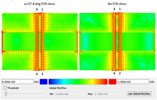
Figure 13 Example of how differential return current behaves on the reference planes when differential 26.3 ps intra-pair skew is introduced (left) compared to no skew case (right).
Finally the last argument to address is the one that says if there is an adjacent ground plane with a very thin dielectric between it and the split power plane, it would act as a better return path across the split. Logically this makes sense from a signal integrity perspective because the impedance of the traces will be reduced in proportion to the thickness of dielectric between the trace and reference plane across the split.
In our previous example we assumed a 4 layer board 0.062 inch thick. That pretty much dictated the thickness of the inner core dielectric layer of the stackup. In order to move the reference plane across the gap closer to the power planes, the PCB layer count needs to increase to minimum 6 layers to maintain a symmetrical stackup and 0.062 inch thickness.
If we reduce the thickness of dielectric under the gap and resimulate the 5 mil gap scenario, we can see the results summarized in Figure 14 when one trace is driven single-ended. The thin dielectric was chosen to be 2 mils; representing a common thickness for buried capacitance core laminates often used for power plane decoupling. When added to the 5 mil thickness, H1 and 1.2 mil thickness of the power plane, L2 shown in Figure 1, we get 8.2 mils total dielectric thickness under the gap.
On the left we observe that most of the return current gets diverted around the gap on reference plane L2. On the right, we see much of the return current flows under the trace on reference plane L3 when the signal crosses the gap. But there is still some current that gets diverted around the gap on L2 reference plane, and thus will still radiate some noise.
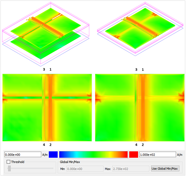
Figure 14 Example of how SE return current density behaves on the reference planes when dielectric thickness is reduced under the gap. On the left most of the return current gets diverted around the gap on L2. On the right much of the return current flows under the trace on L3 when the signal crosses the gap. But there is still some current that gets diverted around the gap on L2 reference plane.
From a signal integrity perspective, the amount of reflection and NEXT was reduced to almost a half, as shown in Figure 15 . There was less risetime degradation of the transmitted signal and FEXT was also improved.
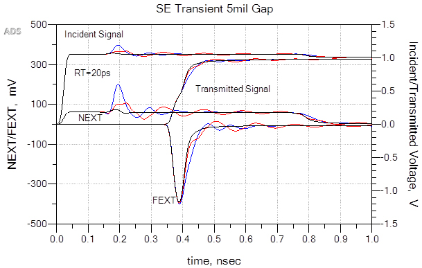
Figure 15 Comparison of SE Incident/Transmitted voltage, NEXT/FEXT for 5 mil gap. Thick dielectric (H2=45 mils blue plots), thin dielectric (H2=2 mils red plots) compared to no gaps (black plots). As expected the closer proximity of L3 results in less incident reflection and NEXT while minimizing risetime degradation in transmitted signal and FEXT.
Summary and Conclusion
So getting back the original debate, who is right? Well it turns out both sides are a bit right. In this paper, several scenarios of signals crossing a split plane in microstrip geometries have been explored. From a signal integrity perspective it appears that a microstrip trace crossing a split plane may be ok within certain caveats. For the examples simulated in this study, as long as the gap between the split planes was minimized to 5 mils, and very thin dielectric was used for power ground adjacent layers, there was no appreciable increase in crosstalk. Depending on your noise budget you might be able to get away with it.
But in terms of passing EMC, there is still more risk and doubt. There was never a scenario where a portion of return current would never flow along the edges of a split in the reference plane, and thus there is still risk of EMI. Because actual designs have many interdependencies affecting the final performance, it is difficult to come up with a general rule that says if you do this, and minimize that you will be ok in every case.
As a general rule for microstrip topologies, it appears the best practice to follow is to still stay away from crossing split planes. When you can’t a more detailed analysis should be done based on the actual layout and stackup of the board; or look for other alternatives that can mitigate noise radiation; like adding extra external shielding for instance.
In the end it is what I always like to say about engineering, “it’s what you don’t know you don’t know that can ruin your day.” What this paper tries to highlight is that in today’s high-speed designs we can no longer restrict our thinking in terms of signal integrity, power integrity or EMC alone. We must consider all three disciplines and become educated or at least aware of each of them. Had we only been concerned about signal integrity, without being aware of EMC we would have probably made the wrong conclusion, and in the end the final product might well have failed EMC compliance tests.
References
- Keysight Advanced Design System (ADS) [computer software], (Version 2016: http://www.keysight.com/en/pc-1297113/advanced-design-system-ads?nid=-34346.0&cc=CA&lc=eng
- PCI Express® External Cabling Specification, Revision 1.0, January 4, 2007