
The frequency content of digital signals in PCB interconnects increased up to 40-50 GHz in recent years. To ensure that interconnects work as expected over this bandwidth, we have to build validation boards. This paper reports lessons learned from validation projects with the goal to build a formal procedure for systematic prediction of interconnect behavior up to 40 GHz. We will discuss the selection of test structures, connectors and measurement equipment, demonstrate uncertainties of the analysis based on the initial pre-manufacturing assumptions, and analyze how closer to reality we can get with a more formal approach based on identifying material models and manufacturer adjustments.
What does it take to design PCB interconnects with good analysis-to-measurement correlation up to 40 GHz? Is it doable with typical low-cost PCB materials and fabrication process, typical trace width, via back-drilling and the shortage of space to place the stitching vias? Your EDA vendor shows excellent correlation of the analysis tools to measurements even up to 50 GHz, your PCB fabricator ensures that the board will be built as designed and provides all possible information on stackup and materials. Measurements with the easy-to-use TDNA or VNA should be also a “piece of cake.” There is nothing to worry about and the designed interconnects should behave as expected.
Unfortunately, many SI engineers quickly learn that this is not the case, and the reality can be far from our expectations. To verify practically everything that goes into the design–to-manufacturing flow at this frequency bandwidth, we are actually forced to build validation boards. Moreover, re-validation has to be done every time a new PCB material or even a new batch of materials or PCB fabricator is used. The outcome of such validation should be a formal process, following which we reduce the gap between the expectations and reality and are able to reliably predict behavior of the interconnects on production boards over this bandwidth. That is the main goal of this project. We do not just show the final analysis-to-measurement correlation on a case-by-case basis, as is usually done in some validation projects, but report a formal procedure based on the material model and manufacturing adjustments identification. The accuracy of the analysis based on the pre-manufacturing assumptions is analyzed and reported. We also discuss un-expected artifacts encountered in the board design, fabrication and measurements (as we all know, stuff happens).
We start with the description of the “dream validation project” – how validation process should look if everything goes as expected. As the framework, we use a “sink or swim” validation process that was developed and tested with multiple validation boards, such as Teraspeed’s PLRD-1 [1], Wild River Technology’s CMP-08 and CMP-28 [2], [3], and Rambus’s “lessons learned” board [4]. The project described in this paper can be considered as the first detailed report of the “sink or swim” methodology application for a board with structures close to the production boards.
We proceed with the validation board planning and discuss selection of test structures. In addition to single-ended and differential transmission line segments for the material parameters identification and test structures like Beatty standards, the board includes common high-speed PCB interconnect structures, such as AC-coupling capacitors, delay matching compensation, meandering line used in DDR circuits, differential and single-ended vias with different number of stitching vias to investigate the energy localization phenomenon. As it is usually done, all structures are designed with the stackup geometry and material parameters provided by the PCB fabricator (pre-manufacturing assumptions).
Next, we show that the bandwidth of the models based on the data available from manufacturer is very limited. Practically, for the target frequency bandwidth it is not possible to predict the interconnect behavior using just the pre-manufacturing assumptions. What would be the minimal possible adjustment to the process to increase the prediction bandwidth and improve the accuracy? First of all, we validate the geometry of the traces with the cross-sectioning. With a few cross-section samples we make new assumptions that the identified trace width and shape adjustments are common for the whole board. Next, we use two transmission line segments (single-ended and differential) for each signal layer to properly identify the material models with GMS-parameters [5]. Finally, with the new set of post-manufacturing assumptions based on the limited board cross-sectioning and on S-parameters measurements for just t-line segments, we go structure by structure and compare the improved models with the measurements. That reveals additional expected and un-expected surprises. The outcome is a relatively simple formal process with a set of recommendations for those who want to design predictable interconnects for validation projects as well as for the production boards.
“Sink or Swim” validation process
One of the key elements of design success is the systematic benchmarking of manufacturing, measurements, and modeling. Systematic means analysis-to-measurement correlation observed not just for one or two structures (test coupons for instance), but rather for a broad range of typical interconnects – single-ended and differential, strip and micro-strip, simple planar and with the vertical transitions or vias, etc. Such comparison should be done consistently both in frequency (magnitude and phase of S-parameters) and time (TDR and optionally eye diagram) domains. In other words, the systematic validation or benchmarking is needed to make sure that the board is manufactured as designed, measurements are taken properly and, finally, that the interconnect analysis software provides acceptable accuracy. It is a huge project, especially if you do it the first time without much experience. Fortunately, there are a number of reports about similar projects to follow [1]-[4]. Here we will use the “sink or swim” approach [4] as the basis. It can be divided into seven steps (including board design and manufacturing):
1. Select materials and define PCB stackup with the manufacturer
2. Design test structures with EM analysis (simple links, launches, vias, etc.)
3. Manufacture the board and mount the connectors
4. Measure S-parameters and validate the quality of the measurements with formal quality metrics and visual inspection
5. Cross-section the board and identify the manufacturing adjustments (if any)
6. Identify broad-band dielectric and conductor roughness models with GMS-parameters or SPP Light techniques;
7. Simulate all structures with the identified or validated material models and confirmed adjustments consistently and compare S-parameters and TDR with the measurements (no further manipulations with the data or “calibration” are allowed at this step);
The initial expectation was to finish the project within 3 months. This was easier said than done – with the low priority and low resources this project took about a year to complete and we are still investigating the data in preparation for yet another iteration. The major hurdle in this project was actually the measurement equipment. Unfortunately, the knowledge of what measurement equipment works for extremely broadband SI problems and what is not suitable is not common knowledge and vendors are not always very helpful,.
Validation board design
A validation platform is very important tool to pre-qualify a manufacturer, benchmark signal integrity software, or to learn how to do the measurements at the microwave to millimeter wave frequency bandwidth. Accuracy and limitations of the software can be easily identified with the analysis-to-measurement comparisons on a typical set of interconnect structures. A validation platform can be either developed in-house or purchased from a vendor. One of the industry-first validation platforms was the physical layer reference design board (PLRD-1) from Teraspeed Consulting Group [1]. Use of the PLRD-1 revealed the need and enabled development of the industry-first broadband dielectric and conductor roughness models in Simbeor software.
An example of a readily available validation platform is the CMP-28/32 channel modeling platform from Wild River Technology featured in [3]. Off-the-shelf validation platforms are convenient tools to learn, but the stackup and interconnect geometry in such platforms may be not be representative for a production board. Custom validation platforms with the stackup structure similar to a production board have to be used in such cases, as it is done in this project.
The board design starts from the material selection and stackup definition. Panasonic Megtron6 material was selected for the high-speed routing layers. Some pre-manufacturing specs provided by the board fabricator are shown in Fig. 1. The board has 20 layers with 8 layers assigned for the high-speed signals as shown in Fig. 2. The target impedance has been specified for the PCB manufacturer , and the manufacturer has to fulfill it with some tolerances. This is the usual choice for a production board. The manufacturer provided expected trace width and spacing adjustments as shown in the right table in Fig 1. The expected impedance variations are within 8%, that is too large to expect good correlation up to 40 GHz, but it is typical value. Vias with 0.20mm (7.9 mil) padstack in board layout are to be drilled with 0.250mm diameter drill (9.85 mil). Non-functional pads on signal vias on any layer are not allowed. Via backdrilling is to be done for some structures.
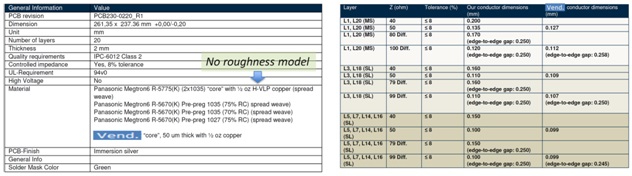
Figure 1. Validation board materials and trace widths and adjustments obtained from manufacturer.
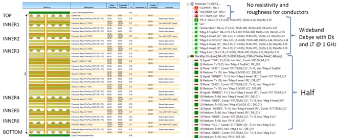
Figure 2. Validation board stackup (left) and the initial material models in Simbeor software (right).
Stackup for the pre-layout analysis was defined as shown in Fig. 2 on the right side. This is the best we can do at this stage. Megtron6 specs provide dielectric constant and loss tangent at multiple frequencies. It is expected that the Wideband Debye (aka Djordjevic-Sarkar) model defined with any of the point from specs provides a good approximation over the target frequency bandwidth. The major problem is with the conductor roughness model: all we know is that the copper foil roughness is specified as H-VLP and no other data. The PCB manufacturer also roughens the shiny side of the copper foil during the board manufacturing, without any parameters for the electrical modeling. Even if we would have data for the mate side of the copper foil from the copper foil manufacturer, the PCB manufacturer treatment of the shiny side makes it practically useless. Thus, we start without the conductor roughness model and with the trace adjustments provided by the PCB manufacturer. Obviously, this will not provide good correlation for the insertion loss and the model identification is needed – this should be expected. Though, the data may be acceptable for design of launches and vias. Ideally, a test coupon with the same stackup should be built for the material identification, to identify the conductor surface roughness model, and to improve accuracy of the pre-layout analysis. The validation board may be considered as such coupon.
The structures on the validation board should include structures for the material model identification and validation. For identification with GMS-parameters [5] or SPP Light [6], two segments of differential or single-ended t-lines for each unique layer have to be used. In addition, we can use Beatty standard (series resonator) to confirm that the extracted models work for traces with different widths. The line segments used for the material identification can be also used as tests for simple differential and single-ended links (they are similar to the traces used on production boards). In addition, we decided to put structures usually used in interconnects for the serial and parallel interfaces: differential and single-ended (SE) via-holes for each routing layer; AC coupling capacitors similar to those used on SERDES links; meandering line segments similar to used on DDR links; and differential link skew compensation structures. All are routed at an angle to the edge of the board to avoid the fiber weave effect. The final board layout with all structures is shown in Fig. 3 and Fig. 4.
The most important elements of the validation board design are the launches. Launches for either probes or connectors have to be optimized. If launches reflect too much, it usually makes them more susceptible to manufacturing variations and more difficult to de-embed for the material identification. The design target is to minimize the reflection and the sensitivity to manufacturing variations. The board is designed to have either 2.92 or 2.4 mm compression-mount connector mounted on the TOP layer. Connectors from two vendors were used. Five low-reflection launches were designed to connect TOP and BOTTOM for structures with microstrip lines, TOP to INNER1 (with backdrilling), TOP to INNER2 (with backdrilling), TOP to INNER3 (with backdrilling), and TOP to INNER6 (no backdrilling). Stackup/materials obtained from the manufacturer are used to simulate and optimize the launches.
Examples of the launch designs are shown in Fig. 5 and 6. The launches are simulated and optimized using a de-compositional approach without connectors – it degrades the model quality and the models are expected to work only up to 30 GHz. All launches are designed with 9 stitching vias located on a circle with diameter 2.3 mm (91 mil). Stitching vias connect all reference planes together with the metal patches in the TOP layer. Stitching vias have drill hole diameters of 0.250 mm (9.85 mil). Distance from signal via to stitching vias is about quarter of wavelength at 30 GHz (quarter of wavelength in dielectric is about 1.35 mm) – it is expected that the launches should gradually lose the localization at about 30 GHz (the impedance of the short circuiting vias at a quarter wavelength distance becomes very high, close to open). We cannot expect good correlation above that frequency. Though, it is expected that the impedance of the return path will remains low due to large parallel planes and plenty of stitching vias placed along the t-line segments.
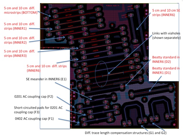
Figure 3. Layout of 20-layer validation board (red legends are for the material identification structures).
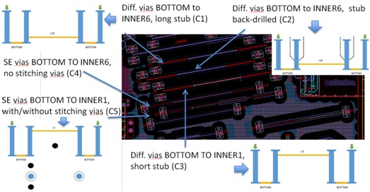
Figure 4. Layout of links with single-ended (SE) and differential viaholes.
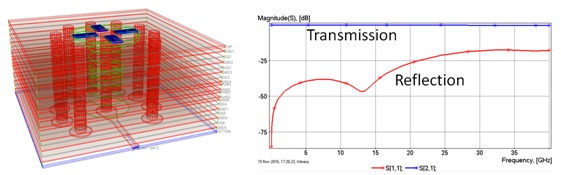
Figure 5. TOP to BOTTOM layer launch design for microstrip structures – the reflection loss is below -20 dB up to 27 GHz and below -10 dB up to 40 GHz.
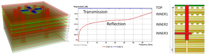
Figure 6. TOP to INNER3 layer launch design for strip line structures in layer INNER2 – the reflection loss is below -20 dB up to 33 GHz and below -10 dB up to 40 GHz.
After the board was designed and sent to manufacturer, we noticed that the metal traces were put in the TOP layer as is visible on Fig. 3. Fortunately, that did not matter because the TOP layer was isolated from all traces on the board by the solid metal plane. At the end of the board layout stage, we made the following reality observations:
- Via diameter is defined 0.2 mm (7.9 mil) in layout file, but 0.25 mm (9.85 mil) is supposed to be used by the manufacturer – it should be accounted in the post-layout analysis;
- The PCB is manufactured with the “impedance control” process – all trace width and spacing are adjusted by the PCB manufacturer, that is also not reflected in the layout file, but should be accounted in the post-layout analysis;
- No information on trace shape (important for the losses evaluation);
- No information on solder mask shape/parameters;
- No information on conductor roughness model;
- No information on actual backdrilling;
All of this makes the post layout analysis not accurate and practically useless at the target frequencies. This is mostly because of the absence of conductor roughness models. It is expected that the HVLP roughness and additional copper processing by the manufacturer substantially degrades the signal above 3-5 GHz, but we have no data to evaluate these additional losses. This should be expected in any project without the test coupons built upfront and exactly the same materials and manufacturer. However, the dielectric parameters and stackup structure from the manufacturer may be acceptable to design the vertical transitions.
Measurements and GMS-parameters extraction
The main goal during the measurement step is to have accurate, high-quality S-parameters measured from 10 MHz to 40 GHz. Considering the manufacturing variations and launches localization, the S-parameters should be suitable for the extraction of the reflection-less generalized modal S-parameters (GMS-parameters) for the material parameters identification [5] up to 30 GHz. Achieving that goal is the most challenging and lengthy step of this project.
The board was manufactured as scheduled, and the S-parameters were measured first with TDNA as shown in Fig. 7. The formal quality metrics of these S-parameters was barely acceptable (as shown on the right side of Fig. 7). Though, the visual inspection revealed a significant amount of noise that is clearly visible on the S-parameters magnitude plots shown for just two structures in Fig. 8. That level of noise may be acceptable for a preliminary validation. However, the GMS-parameters [5] computed with these S-parameters were also very noisy, as illustrated in Fig. 9. We were faced with the choice to either proceed with this noisy data or find other options.
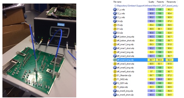
Figure 7. S-parameters measurement setup with TDNA (left) and final Simbeor quality metrics (right, IEEE T370 PG3).

Figure 8. Example mixed-mode S-parameters measured with TDNA for differential 10 cm segments in layers INNER1 (strip, left) and BOTTOM (microstrip, right) – acceptable quality metrics, but noisy.
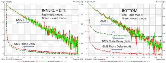
Figure 9. GMS-parameters computed with S-parameters measured with TDNA for 5 cm differential strip lines in layer INNER1 (left) and 5 cm diff. microstrips (right) – may be acceptable up to 10 GHz.
If we proceeded with the noisy GMS-parameters, the material identification would be ambiguous above 10 GHz. This was unacceptable. So, we decided to find other measurement options, including attempts with a 26-GHz VNA, multiple 40-GHz VNAs, and a 50-GHz VNA.