
Reader beware: this article is yet another that illustrates the true nature of bends on circuit board traces by measurement and simulation.
Bends in PCB traces look like very basic, simple structures that are easy to simulate. Technically, one can do the analysis with any electromagnetic solver with sufficiently accurate port de-embedding capabilities [1]. The reflections from a bend in fine-line, high-speed digital interconnects are relatively small and may not even be detectable with measurement. So, who cares?
Surprisingly, my recent LinkedIn post on how to minimize the reflections from the bends generated a lot of interest and questions. The bend effect may be negligible in fine-line digital interconnects, but not so in wider traces used in RF/microwave structures that nowadays are often implemented on two-layer PCBs. The analysis of bends in thicker dielectric substrates with wider traces is more important in RF applications.
At a recent EPEPS conference, Jose Moreira and his team at Advantest demonstrated excellent measurement- simulation correlation on the bend geometries in test boards [2]. He also suggested correlating the measurements done at Advantest with the analysis in Simbeor and provided all necessary measured data for structures shown in Fig. 1 – an excellent opportunity to validate electromagnetics with measurements (or the other way around).
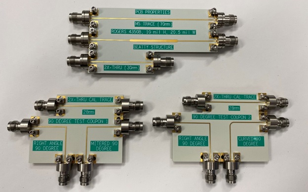
Fig. 1. Test structures from Advantest for material model identification (top) with uncompensated and mitered bends (bottom left) and uncompensated and curved bends (bottom right).
The first step is to identify the material properties. This is an essential step to achieve close mesurement- simulation agreement in any project. The material identification can be done using S-parameter measurements for long and short lines (top structure in Fig. 1) with the reflection-less GMS-parameters [3] in Simbeor software.
S-parameters were measured up to 60 GHz by Jose Moreira. All quality metrics of measured S-parameters came out as good or acceptable and TDRs of two line segments were consistent for the material model identification up to 60 GHz.
All test structures are microstrip lines plated with thick layers of nickel (assumed as typical 6 um) and relatively thick layer of gold (assumed 0.1 um – thicker than usual). That plating is important to account in the model - it produces substantial effect on the losses. We know properties of Rogers 4350B dielectric from manufacturer (may be a starting point in the material identification) and can take Landau-Lifshits model for nickel from [4].
The unknown here is mostly the roughness model parameters. The outcome of the identification is the models with parameters shown in Fig. 2 – that produces correlation in GMS-parameters shown in Fig. 3. (To capture the high-frequency dispersion, the Simbeor 3DML solver was used for all simulations in this paper.)

Fig. 2. Material models and stackup. Roughness is specified for rough surfaces of copper in stackup as Huray-Bracken model with SR=0.6um and RF=8.
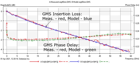
Fig. 3. Measured and modeled reflection-less GMS transmission parameter for 20.5 mil wide, 40 mm segment of plated microstrip line (difference of long and short line) after adjustments of the material models.
The next step is to create models of the bends and correlate with the measurements. TDR responses computed from measured S-parameters of the bends are shown in Fig. 4 (computed with rational compact models (RCM) in Simbeor). This is a straightforward time domain simulation using the RCM models. The effect of the bends is quite visible in the TDR responses due to the wider than usual traces and the very short rise time in the TDR simulation.
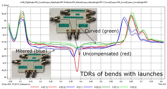
Fig. 4. TDRs computed from measured S-parameters for three test structures from the opposite ends.
The uncompensated bend has an almost 4 Ohm dip (red lines), mitered bend has a little over 1 Ohm dip (blue lines), and the curved one has less than 0.5 Ohm dip (green lines). The bend’s dips are in the middle of TDR graphs. All bends add capacitance.
Also important to note, is that the real structures have substantial manufacturing variations – about 1 Ohm along the traces and about 1.5 Ohm in the launches. This variation in the actual as-manufactured properties of the test structures will fundamentally limit the measurement-simulation agreement.
There are two ways to proceed with the model building and comparisons. The first way is to create models for the whole structures, including the connectors and launches. This is possible, but it requires geometry or models of the connectors and is more complicated to setup.
Another option is to de-embed the connectors and launches using a 2x thru reference structure and extract measured S-parameters for just the bends with small segments of traces on both sides. De-embedding is a way to subtract the effect of connector, launch, and some trace segment from the original S-parameters. That leaves S-parameters only for the structure under investigation (bends in this case).
Identified S-parameters of half of the 2x through structure can be used for such subtraction. That is what was done in [2] using the AFR de-embedding method (see details in the paper). Jose Moreira provided measured and de-embedded S-parameters as well. Geometry of each bend was imported into Simbeor software from the ODB++ file together with materials and stackup data from the material identification project (Fig. 2).
After de-embedding, the reference planes on both ports were moved to either side of the bend region. Rational compact models were computed for each bend structure that allows direct computation of the time domain TDRs for each bend. The de-embedding in [2] was done with the 2x through structure – half of the length of this structure gives the location of the post de-embedded reference planes. Simulation of the bends is really simple to do from the ODB++ data file. The measurement-simulation comparisons of TDR and S-parameters are shown in Fig. 5 – Fig. 10.
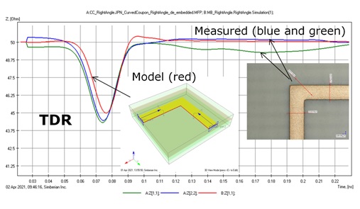
Fig. 5. TDR computed from measured and de-embedded S-parameters and from modeled S-parameters of uncompensated bend.
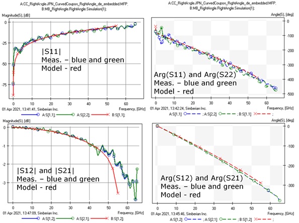
Fig. 6. Magnitudes and angles of measured and modeled S-parameters of uncompensated bend.
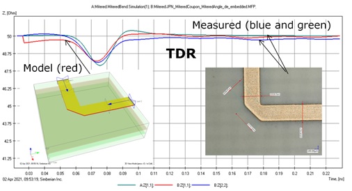
Fig. 7. TDR computed from measured and de-embedded S-parameters and from modeled S-parameters of mitered bend.
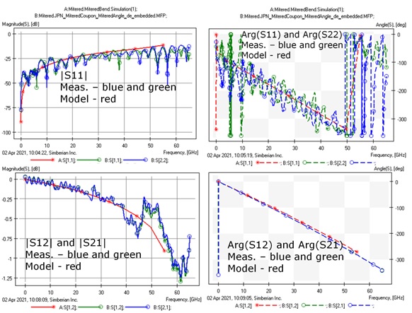
Fig. 8. Magnitudes and angles of measured and modeled S-parameters of mitered bend.

Fig. 9. TDR computed from measured and de-embedded S-parameters and from modeled S-parameters of curved bend.

Fig. 10. Magnitudes and angles of measured and modeled S-parameters of curved bend.
How good is the measurement-simulation correlation? Overall we can conclude that the correlation is good for uncompensated and mitered bends with higher reflections (Fig. 5 – Fig. 8). Correlation of reflection parameter for the curved bend is not as good and the reason for that is the problem with de-embedding.
Notice that all the measured de-embedded S-parameters have some oscillations in both magnitudes and phases and computed S-parameters are smooth. Are those oscillations physical?
In this case it is a problem with de-embedding due to geometry or material property variations in the test fixtures. The variations in the launches and traces are clearly visible on the measured TDRs in Fig. 4 as well as in Fig. 11.
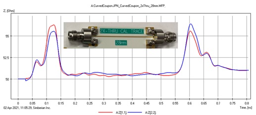
Fig. 11. TDR of 2x-through structure from the opposite end computed from measured S-parameters – shows violation of symmetry and differences with the de-embedded structures.
When S-parameters of the 2x through structure are divided into S-parameters of two halves, those halves are not exactly the same as the transitions to be removed in the structures with the bends. Thus, when subtraction is done, the differences show up as the ripples. The de-embedded S-parameters have acceptable quality and can be easily converted into passive and causal rational compact macro-models for the TDR computations for uncompensated and mitered bends.
However, it was not possible to reasonably fix the S-parameters for curved bends with the reflections below -20 dB. The noise introduced by physical differences in test fixtures was comparable with the effect of discontinuity in this case.
Conclusion
This simple experiment demonstrates the measurement-simulation correlation possible in well-engineered PCB structures. High quality measurements were done by Advantest with state of the art de-embedding. Good analysis to measurement correlation was demonstrated for relatively reflective bends – uncompensated and mitered (with not so optimal positon of the cut). The measurement-simulation correlation is still close, but not as close for the curved bend, due to the very small impact from the curved bends, of comparable magnitude to the manufacturing variations in the test fixtures.
References
-
Y. Shlepnev, How Interconnects Work: How Interconnects Work: Minimal-reflection 90-degree bends in strip lines, Simberian App Note #2021_01, March 2, 2021
-
H. Barnes, G. Bianchi, J. Moreira, A Review of 90 Degree Corner Design for High-Speed Digital and mmWave Applications, IEEE EPEPS 2020, https://ieeexplore.ieee.org/document/9231371
-
Y. Shlepnev, Broadband material model identification with GMS-parameters, IEEE EPEPS 2015
-
Y. Shlepnev, S. McMorrow, Nickel characterization for interconnect analysis. - Proc. of the 2011 IEEE International Symposium on Electromagnetic Compatibility, Long Beach, CA, USA, August, 2011, p. 524-529.