
Obtaining accurate measurement data requires either accurate knowledge and accounting for the probe and fixture influence OR calibration methodology to remove these effects prior to measurement. Vector network analyzer (VNA) users perform a complete calibration of the measurement setup and fixtures before making measurements. This process assures accurate measurements, with artifacts due to the setup removed, or de-embedded.
Oscilloscope users can also calibrate their passive oscilloscope probes, though the process is much less sophisticated and for lack of a better term, wrong. The calibration process also generally can’t include the "fixture.” This short article shows you what to measure and a method to accurately measure the response of the probe. In addition to the probe, there are other errors that need to be removed. Most importantly, this article will show you how to accurately measure the passive probe response.
Probe frequency response
Ideally, an oscilloscope has a flat response up to the bandwidth of the probe, followed by a single pole response, which is -3dB at the probe bandwidth.
Typical passive oscilloscope probes offer between one and three compensation adjustments in order to achieve the desired flat response. Most oscilloscopes also provide a pulse calibration signal that is used as a signal source, which is used in conjunction with the oscilloscope probe to display the pulse on the oscilloscope. The probe compensation adjustments are then used to achieve flat response and correct signal amplitude. Unfortunately, there is a fallacy in this process, and the results aren’t as good as you might think. Here’s why:
Anatomy of an oscilloscope probe tip
The oscilloscope probe is made up of a metal tip and an internally compensated, high impedance voltage divider. This then connects to the compensation adjustment capacitors and on to the probe cable and ultimately to the connector that mates with the oscilloscope.
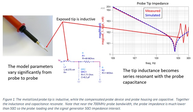
A typical oscilloscope tip is shown in Figure 1. The exposed tip is inductive, while the compensated voltage divider and scope barrel present a capacitive impedance. Measuring the impedance tip using a VNA, we can directly measure the capacitance and tip inductance. The inductance and the capacitance combine, forming a series resonance at a frequency that can be calculated as:

In this probe, the resonant frequency is about 700MHz.
So, what’s wrong with the way we calibrate oscilloscope probes?
Performing the oscilloscope probe calibration using the pulse source imposes three very simple requirements:
- Since the signal voltage is not monitored at the probe tip, the signal generator impedance must be small compared with the impedance of the probe tip (10dB is a reasonable minimum separation)
- The calibration signal must have flat frequency response
- The calibration signal rise/fall must be above the bandwidth of the probe (10dB is a reasonable minimum separation). The rise/fall time can be calculated as:

Allowing for the 10dB minimum separations requires the calibration to be performed using a flat response generator with greater than 2GHz bandwidth (700MHz +10dB), 170ps rise/fall time (500ps – 10dB) and 630mOhm source impedance (2Ω -10dB).
Unfortunately, the calibration signal generator is a 50Ω signal and generally with an edge speed significantly below the 170ps required. Because we aren’t able to accurately calibrate or de-embed our probe, our data can be significantly impacted, or in other words, wrong.
We need a different method to accurately measure the probe
The first requirement can be resolved by measuring the voltage at the scope tip as well as at the back end. This eliminates the need for a 60mΩ signal generator impedance. The second requirement of wide bandwidth and flat response can be met using a low repetition rate, fast edge impulse generator. The frequency response of an impulse signal is very flat up to a bandwidth determined by the rise/fall time, as in equation (2).
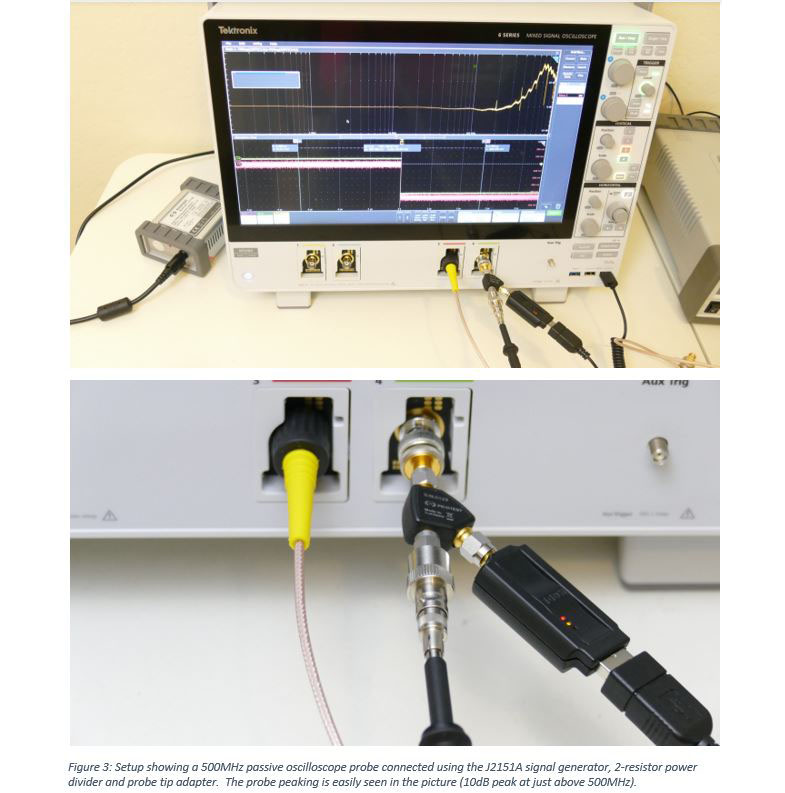
In the following example I’m using a Picotest J2151A pocket sized signal generator, but any equivalent flat response fast signal generator can be used. The rise/fall time of the J2151A are about 34ps, and NIST traceable calibration data shows -3dB bandwidth of 10.5GHz and 0.1dB flatness at 700MHz.
The J2151A includes a 15GHz, 2-resistor power divider that is the key to measuring the probe tip voltage. The setup picture in Figure 3 shows the signal generator and 2-resistor power divider. The probe is connected using a probe tip adapter (not included) and the setup picture is shown in Figure 3.
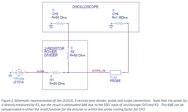
While the signal generator is 50Ω, one leg of the power divider connects the probe tip to a 50Ω oscilloscope input (CH3). This connection attenuates the tip voltage by 6dB, which is corrected in the probe parameters, but also allows full bandwidth of the channel. The probe output at CH4 measures the voltage at the back end of the probe.
The voltage spectrum of the probe backend voltage divided by the voltage spectrum of the probe tip voltage provides the probe transfer function, independent of the tip loading. The probe delay is also seen as the delay between the input and output oscilloscope traces (CH3 and CH4 respectively).
The probe tip impedance, desired for de-embedding can be obtained from a VNA as shown in Figure 1, but can also be derived from the voltage spectrum response at CH3. Alternatively, it can be estimated using the typical probe tip capacitance from the datasheet.
A few more obstacles
While this measurement provides an accurate response using a probe tip adapter, the addition of a ground lead will also significantly impact the response. This lead is difficult to account for, since it is flexible, and therefore the inductance will vary if the lead is moved. The measurement should be made in a configuration close to the actual measurement.
An additional issue is that often the circuit being probed includes a probe tip adapter or header. These include PCB traces connecting to the signal being measured. These traces add additional inductance, that appears in the same way as the probe tip inductance. These traces also include delays that should be included for accurate deskewing or de-embedding of the probe.
Flattening the peak
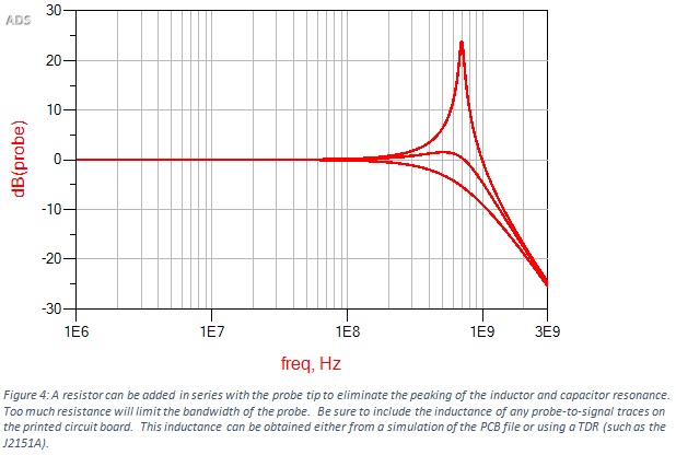
The peaking of the scope probe can be damped by inserting a resistor in series with the probe tip. The value of the resistor is estimated from the tip and PCB trace inductance and tip capacitance as shown in Equation 3.

This additional resistor can significantly flatten the probe response, though it can also reduce the bandwidth of the probe. The impact of the resistor is shown in Figure 4 using the probe from Figure 1. Without the resistor the probe shows peaking of approximately 25dB. The addition of a 40Ω resistor achieves near flat response, while inserting an 80Ω resistor overdamps the response and reduces the probe bandwidth.
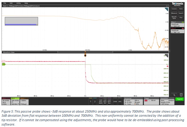
Not all probes can be easily corrected. A simple inductor and capacitor resonance can be damped using a series resistor, but not all probes present such a response. The probe response shown in Figure 5 shows non-uniform flatness, but not a discernable peak that can be damped. If this non-flat response can’t be compensated using the adjustments, the probe must be de-embedded using post processing software, or the usable bandwidth of the probe is greatly reduced.
This methodology applies to active probes as well
Active probes present a much smaller tip capacitance which helps to achieve flat response, but the higher bandwidth also presents challenges in the signal generator requirements.
Consider a typical active probe with a maximum specified tip capacitance of 1pF. Measuring the probe response by connecting to a 50-Ohm source results in a bandwidth limit of:

Applying our 10dB rule, this would only allow measurement to about 1GHz while achieving this. Measuring a 4GHz power rail probe requires measuring the tip voltage and using a signal with an edge speed of about 12GHz. The J2151A is a bit slow for this, but will provide decent, though not as accurate results.
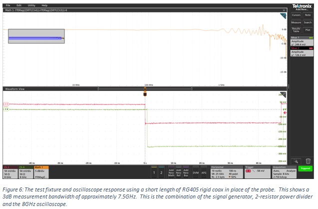
The flatness of the setup can also be evaluated by replacing the probe with a short length of high quality, high bandwidth coax cable. The results of this evaluation are shown in Figure 6. The results are flat with some ripple above 1GHz and a 3dB bandwidth of about 7GHz. This is consistent with the 10GHz scope bandwidth, which would be somewhat reduced by the 10.5GHz signal generator.
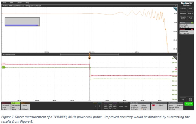
Replacing the coaxial cable with an actual active probe, in this case a TPR4000 power rail probe, results in the measurement shown in Figure 7. To achieve improved accuracy, the measurement of the short coaxial cable should be subtracted from the probe measurement, though even the direct probe measurement shows a 4GHz bandwidth.
Summary
The probe tip and inductance have a significant effect on the performance of the probe. Measuring the probe, directly, using a 50Ω signal is inadequate in all but a few cases. Two other lessons are that while we often do need to use the probe close to its bandwidth, it is essential to know the probe (and oscilloscope) response to get accurate answers. Also, this excess tip inductance is also introduced as printed circuit board traces to get the signals to a convenient probing location. These printed circuit board traces will also impact this probe response and the probe peaking. In the future, possibly the oscilloscope manufacturers will add calibration and de-embedding for this measurement.
The method shown here uses a fast edge signal generator, the oscilloscope, and voltage spectrum division as a VNA to measure the frequency response of the probe. There are still errors, for example, even the scope probe tip adapter adds some inductance. The oscilloscope itself isn’t perfectly flat up to the rated bandwidth of the oscilloscope.
Next, I hope to perform a high-speed impulse response measurement using a GaN driver to corroborate these measurements and the method. Maybe in a future article I’ll show how to extract the probe tip impedance from this measurement as well.