

As network speeds have increased, the challenge of meeting eye height and eye width signal integrity metrics has become more challenging. Maximizing these metrics helps achieve the specified bit error rate (BER) at a target baud rate. One area that can be exploited to gain design margin, particularly eye width, is to minimize the jitter and noise of the crystal oscillator (XO) reference clock.
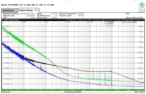
On the surface, picking the XO with the lowest jitter and noise is a simple task since most datasheets provide specifications for jitter and phase noise in terms matched to a variety of applications. These specifications are measured in the vendor’s laboratory with the cleanest power supplies available. See Figure 1 for an example phase noise plot that uses the Epson SG7050EEN 156.25 MHz LV-PECL differential output XO. The results of the 12 kHz to 20 MHz and 40 Hz to 20 MHz integrated RMS phase jitter measurement are highlighted.
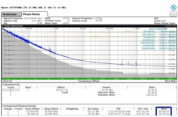
Figure 1 - Baseline Phase Noise Graph with Clean Supplies
Notice that the phase noise plot is smooth and without lumps, bumps, discontinuities, and, most importantly for this article, without spurs associated with the noise and ripple on the power supply. In the actual applications, the power supply ripple and noise in the system increases the jitter and noise of the XO beyond the specified limit since very clean power supplies are used during device characterization.
The spectral content of the ripple and noise on the power supply line directly impacts the shape of the phase noise. For discrete noise, each independent frequency associated with the noise exhibits a spike or “spur” superimposed on the plot. Depending on the XO topology they can distort the phase noise plot’s shape further, see Figure 2 for the 50 kHz spur associated with the injection of 30 mV peak-to-peak on the device under test (DUT) in Figure 1 operating with 3.3V supplies.
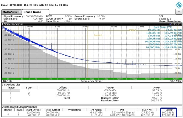
Figure 2- 50 kHz Fixed Frequency PSNR Injection
Notice the increase in the RMS integrated phase Jitter readings with the 50 kHz 30 mVp-p injection. This demonstrates that, since different XOs react to power supply noise and ripple differently, the XO that has the lowest jitter and noise specifications may not be the lowest in the application. What is needed is a test method that a customer can use to select the best XO when applied to their specific situation.
Background:
The correlation between total jitter (TJ) and BER has been well established, see [1] and [2]. TJ can be broken down as the sum of random jitter (RJ) and deterministic jitter (DJ) when in the correct units. RJ and DJ are defined as:
RJ – follows a Gaussian probability density curve and comes from the unpredictable behavior of the timing source. Its amplitude is unbounded. The sources of RJ are related to physical properties of the resonator and design of the XO circuit. Some of these properties may include thermal, or Johnson noise related to fundamental properties of resistors.
DJ – is predictable and does not follow a Gaussian distribution; it is bounded, and its amplitude is fixed. There can be multiple sources of DJ; some are related to the bitstream while others are due to interactions between the components of the system. One example is the interaction between power supplies and the XO’s internal circuits.
The measurement procedure in this article addresses the DJ that comes from the interaction between an XO and its power supply’s voltage ripple and noise. Since the TJ is what determines the actual performance of the XO in the application; the added DJ is one source that can have a significant impact on the system’s TJ. This measurement methodology uses common test equipment to measure an XO’s RJ, DJ, and TJ with power supply ripple and noise applied to enable competitive comparisons.
Solution:
Measurement Method
Conceptually the measurement of PSNR is very simple:
- Set up the test equipment and fixture
- Using a clean power supply, set the DC voltage to the target voltage
- Measure the XO’s baseline phase noise response, see Figure 1 and Figure 2 for an example
- Inject the lowest frequency and set the amplitude to the desired target
- Superimpose a noise-like signal on the power supply
- Re-measure the jitter with the injected noise, see Figure 2 for an example
- Subtract the noise injected jitter from the baseline jitter, the result is the DJ induced on the XO by the extra content of the signal superimposed on the power supply
Measurement Resources
The following instruments will be used:
- Phase Noise Analyzer (PNA) – to measure the jitter
- Oscilloscope (O-scope) – to measure the DC level and AC injection amplitude at the power supply pins of the DUT
- DC Power Supply (DCPS) – low noise DC supply
- Function Generator (FG) – provides the noise stimulus
- XO Evaluation board – provides the appropriate bias and termination to the XO
- Balun – converts differential device output to single-ended instrument input to the PNA
- Power Rail Probe (PRP) – Probe to be used in conjunction with the scope
- Power Line Injector (PLI) – combines DCPS and FG outputs and outputs the results as the DUT’s power supply
Figure 3 shows a schematic of the test setup using the PNA, it is shown pictorially in Figure 4. It is possible to use a real time oscilloscope (RTO) in lieu of a PNA to make this type of measurement [3, 4] however the PNA was chosen due to its low noise floor.
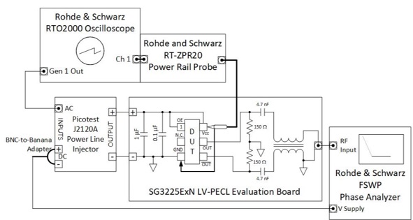
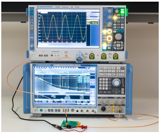
Figure 4 - PSNR Test Setup Picture
Frequency Ranges
Injection Frequency Range:
Lower Bound – holding over from academia and later telecommunication specifications (see [5]), frequency variation ≤ 10 Hz is considered wander and not jitter. This wander is due to ambient temperature variation and other slow-moving effects. Since some XOs use a low frequency resonator and a phase-locked loop to create their high frequency output, low frequency power supply noise can create harmonics at higher frequencies and we want to include the effects of 50/60 Hz noise, this article uses 50 Hz.
Upper Bound – ripple frequencies from DC/DC converters are in the range of 50 kHz to 1 MHz, testing over these frequencies is needed to understand how the XO’s TJ and PSNR react. The upper end may be limited by the test setup’s ability to source enough current to maintain the injection amplitude at higher frequencies as the impedance of the bypass capacitors consumes more current to maintain the same voltage amplitude, this is a limit of the test setup.
Suggested Range – this article uses: 50 Hz, 100 Hz, 200 Hz, 500 Hz, 1 kHz, 2 kHz, 5 kHz, 10 kHz, 20 kHz, 50 kHz, 100 kHz, 200 kHz, 500 kHz, and 1 MHz.
RMS Phase Noise Integration Range – XOs often specify an integration range of 12 kHz to 20 MHz, this comes from networking applications where signal integrity engineers use this as a key parameter for their selection. There are other integration ranges that can be used, some applications care more about “close-in phase noise” and those might use ranges down to about 10 Hz.
The range can be easily changed by entering different integration start and stop limits into the PNA. For this article we will show results for two integration ranges, 12 kHz to 20 MHz as well as 40 Hz to 20 MHz to show how the range selection affects the measurements.
PNA Start and Stop Frequency Range: PNA measurements can take a long time to make, particularly for low offset frequencies. A start frequency below 10 Hz adds measurement time and no data impacted by the injection. Therefore, starting the PNA at 10 Hz is recommended. For the upper limit, use the highest frequency available that includes 20 MHz as this will cover the 12 kHz to 20 MHz integration range.
Injection Amplitude
Nominal Amplitude Selection – the amplitude must be high enough that it is measurable at the Vcc pin. In practice an amplitude of ~1% of the nominal Vcc is a reasonably typical of power supply ripple so 30 mVp-p on a 3.3V supply is used.
Adjusting for Consistent Injection Amplitude versus Frequency – input levels must be monitored and adjusted due to the effects of the decoupling capacitors, the XO input impedance, and the output impedance of the power supply source. As the injection frequency changes, so does the injection amplitude. Small variations vs. frequency are expected (±50 mV for offset and ±5 mV for amplitude) but large variations will affect the results.
Output Termination and Balun Interfacing
Differential output XOs are typically where very low levels of jitter are required, they give a higher Signal-to-Noise ratio then single-ended ones and suit high frequency applications better. In practice the outputs of a differential XO are connected to the differential inputs of the target IC through a termination network that is matched to the output type and frequency of the system. It is important to use correct termination as that impacts the shape of the clock waveform which can cause higher TJ if incorrect. For this reason, the termination design and values are chosen to be the “industry standard” for LV-PECL outputs.
The PNA input is a 50Ω single-ended input so some type of signal conditioning is needed to connect the differential XO outputs to the PNA input. A balun is used following the termination network to convert the differential output of the network to the single-ended input of the PNA.
Measurement Results, Data Reduction, and PSNR Calculation
PSNR is calculated from the results of two measurements using the PNA’s integrated RMS phase jitter test calculation. The first measurement is the “baseline” phase noise with clean power supplies; see Figure 1. It is important to make sure the PNA is setup properly for the carrier frequency, frequency offsets, over- and underflow, and other setup conditions that can affect the readings. It is good idea to capture the phase noise data as a CSV file from the PNA as well as a screen shot of the display for later documentation purposes.
The next step is to start the injection and start measurements at each injection frequency and capture the results of the PNA’s measurement, this is the TJ result. Using the integrated RMS phase jitter results, the PSNR is calculated by subtracting the RJ baseline measurement for the measured result at each injection frequency from the TJ with injection and dividing by the injection amplitude to give units of fs/mV. See Table 1 for an example of testing the Epson SG7050EEN 156.25 MHz XO with measurements and calculations for 40 Hz to 20 MHz and 12 kHz to 20 MHz integrated RMS phase noise.
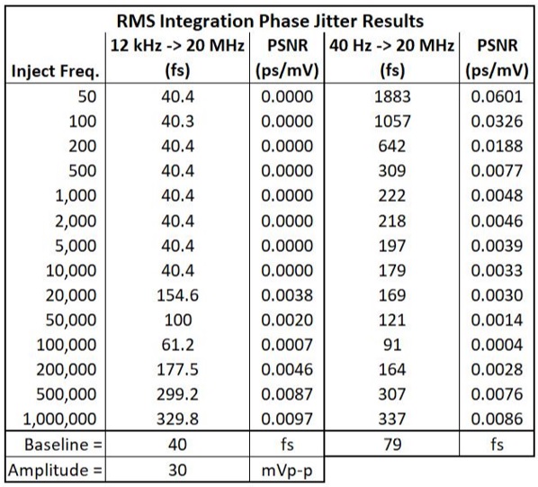
Table 1 - Epson SG7050EEN PSNR Measurement and Calculation Results
Figure 4 plots the TJ and PSNR results of Table 1 versus injected frequency for both integration ranges. Note how flat the 12 kHz to 20 MHz PSNR response is up to the lower bound of the integration compared to the 40 Hz to 20 MHz response. With this XO, the power supply noise does not generate higher-order harmonics, so injections at frequencies below the integration range do not affect the measurement and only the RJ is measured. Once the injection frequency enters the integration range of the PNA, the PSNR shows the anticipated injection spur and gives a measurable PSNR result. This demonstrates the earlier point that it can be useful to inject lower range frequencies and integrate over a wider range of frequencies even for applications that traditionally consider 12 kHz to 20 MHz results in order to see how the XO responds to low frequency power supply noise. Later in this paper we will see a similar measurement for an XO where high frequency content is created from low frequency injection. That difference can be an important consideration in the timing product selection..
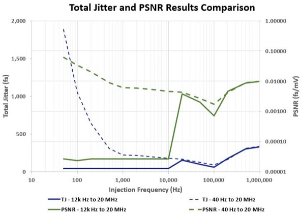
Figure 5 –TJ and PSNR Measurement Result Comparison
Comparing XO Results
This section of the article shows the results of running a baseline measurement on three of Epson’s 156.25 MHz, LV-PECL output XOs to show how to make comparisons. For this we used the SG7050EEN specified for a Phase jitter of 70 fs max. The SG7050EAN is specified for 600 fs max, and the XG2102CA at 180 fs max. The SG7050EAN is an older generation to the SG7050EEN using a low frequency Xtal resonator and PLL to get to the final output frequency while the XG2102CA is a surface acoustic wave (SAW) XO so it uses a very different resonator technology and represents an even older generation of XO. Figure 5 shows the baseline response for each XO, note how different the plots look for each XO, this is characteristic of the type of resonator and design topology of each one.
All three XOs were tested and compared using the PSNR measurement techniques in this article, Figure 6 shows the TJ results that came from those measurements and Figure 7 shows the PSNR results. Note that for this section we are focusing on the Integrated RMS phase noise results from the 40 Hz to 20 MHz in order to show how to use the full range of the test to characterize the full PSNR performance over frequency.

Figure 7 - TJ Competitive Comparison Results

Figure 8 - PSNR Competitive Measurement Results
Comparing the TJ results of Figure 6 to the PSNR results of Figure 7 demonstrates that it is the combination of low RJ and robust PSNR that gives the best performance. This is demonstrated by the lower TJ performance of the SG7050EAN up to 1 MHz as compared to the XG-2102CA. (This is even though the XG-2012CA’s phase jitter specification is 3.3x better.)
Conclusion:
Designers pushing the limits in their application can run into situations where the XO performance is inadequate for their next design due to the way it reacts to the noise and ripple in the power supply. To achieve optimal performance, they most likely will find they will need to do more than a simple datasheet evaluation to select their next XO, the customer may need to test PSNR themselves to find the one(s) that give the lowest TJ for their designs. With the PSNR test method from this article, they can make the measurements to select the XO that gives them the best performance for their money.
References:
[1] Maxim Integrated, “Jitter in Digital Communication Systems, Part 1”, San Jose, CA, Application Note: HFAN-4.0.3, Rev 0, September 2001
[2] Maxim Integrated, “Jitter in Digital Communication Systems, Part 2”, San Jose, CA, Application Note: HFAN-4.0.4, Rev 0, March 2002
[3] Rohde & Schwarz, “Comparison of jitter measurements in the time and frequency domain”, Munich, Germany, Application Card PD 5215.3279.92, Version 01.00, July 2017
[4] Dr. Mathias Hellwig, “Jitter Analysis with the R&S®RTO Digital Oscilloscope”, Rohde & Schwarz, Munich, Germany, Application Note PD 1TD03_2e, Version 01.00, July 2017
[5] National Institute of Standards and Technology, “Characterization of Clocks and Oscillators”, NIST Technical Note 1337, United States Department of Commerce, March 1990