
Propagation phase and phase delay
The first term in (19) describes the phase of the propagation function, which is 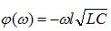 . We can evaluate this value for causal and non-causal models at mid and high frequency (assuming that
  For causal model, we should take “+” in this expression. From here, the difference in phase becomes
  , and the phase delay:
 (22)
(22)
Figure 6. (a) Contribution into phase delay from different types of losses; (b) the difference in phase delay due to roughness causality: simulated (solid) and predicted by (22) (dashed)
Figure 6a shows contribution from different losses into the phase delay. A loss-less transmission line has constant phase and group delay. For a lossy line, an additional delay decreases with frequency and approaches the value defined by capacitance and inductance at infinity. For a given test case, the largest addition comes from impedance of the smooth metal (green), which dominates at low frequency. It decreases approximately as  , as relative contribution of inductance due to skin effect.
Next in importance comes additional delay caused by extra capacitance associated with dielectric loss (blue). This dependence practically repeats the real part of the Djordjevic-Sarkar equation for relative permittivity of dielectric.
Contribution into phase delay from the causal roughness model (red) remains almost constant within wide range. At low frequency, we have  increase of the factor
  . Multiplied by an impedance of the smooth metal, also growing at this rate, it makes a linearly growing contribution that practically stays in constant proportion with
  thus increasing an equivalent inductance and phase delay. Only at a higher frequency, where blue curves in Figure 2b become flat, does this factor settle and its relative contribution diminishes.
For non-causal model (black), the multiplier at inductive impedance  is by orders smaller, and practically not visible. At higher frequency, the red curve in Figure 2b approaches blue, because the imaginary part of the complex correction factor starts to go down and the lack of it becomes less visible. This is where contributions from causal and non-causal models converge.
Figure 6b illustrates the difference in phase delay caused by using the causal model. Solid is simulated, while dashed is predicted by formula (22). The difference slowly decreases but remains considerable up to 50GHz. This is consistent with the red/black curves in Figure 6a.
Characteristic impedance of the line
At sufficiently high frequency  We choose “+” for causal and “-” for non-causal model. By assuming that losses are small and expanding the expression under square root, we find the difference:
 . (23)
A more accurate estimate is possible if we don’t ignore losses but consolidate them in the denominator, as follows:
 (24)
(24)
In this expression, the denominator depends on PUL conductance and impedance. It is mostly imaginary and grows linearly with frequency. Therefore, the surplus in characteristic impedance is mostly real, and decreases as  .
.
Figure 7 shows the difference in characteristic impedance caused by model causality. Red and blue curves are real/imaginary parts of this difference found from two simulations. Green illustrates real part of the difference found by the simplified equation (23). Dashed black and cyan show real/imaginary parts of more accurate evaluation of this difference per equation (24). The latter perfectly matches numerical evaluation.
At low frequency the nominator in (24) grows linearly, the same as the denominator, thus making the difference approximately constant. At higher frequency,  peaks, then starts decreasing, thus making this difference smaller. In our particular case, the difference in characteristic impedance between causal and non-causal models is about 1% compared to ~50 Ohm characteristic impedance. But depending on line’s parameters, it could be larger or smaller.
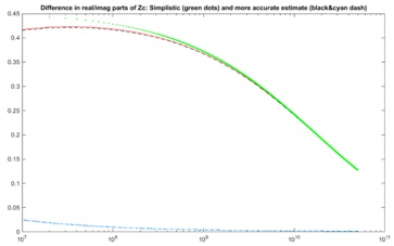
Figure 7. The difference in characteristic impedance of the line due to causality of the roughness model
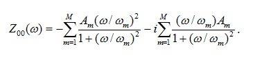
V. Restoring causal correction factor from the loss factor given by a table
Sometimes material vendors describe the loss correction factor by tabulated dependence  given as (frequency, value) pairs. This dependence corresponds to #2 or #6 in Table 1; hence it is a difference between real and imaginary parts of the unknown complex multiplier
  .
.
Since should be a causal dependence, it’s tempting to represent it by a sum of simple rational components, for example as 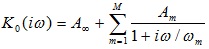 , then equate the table-given dependence,
  to the difference between real and imaginary parts of this representation and then try to find the unknown coefficients. However, this approach fails in most cases because the task becomes ambiguous. Although we can restore a missing real (imaginary) part from a given imaginary (real) part, there is no single solution when restoring the two if we only know the difference between them.
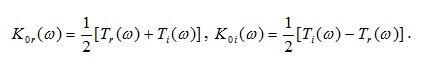
As shown in Figure 8a, the real and imaginary parts of the fitted approximation to  remain uncontrollable outside the data range, even though the loss factor is fitted accurately (Figure 8b). Note that both multipliers in Figure 8b decrease above ~10GHz, which doesn’t match our expectations.
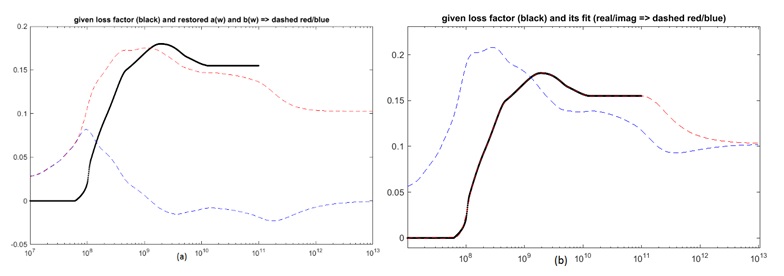
Figure 8. (a) Given loss factor (black), real and imaginary parts of the fit (red/blue) whose difference approximates the loss factor; (b) fitted loss (red) and inductance (blue) correction factors
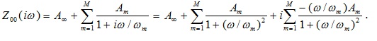
The proper way is to work with complex impedance, for which we can find the real part. For example, a normalized surplus of PUL impedance can be represented as

assuming the complex factor  . Therefore the real part of the surplus impedance should interpolate values
  . Since
  is causal, it can be approximated e.g. by a rational fraction expansion of the form:
 (25)
(25)
To simplify the task, we can choose a set of M (typically 15…30) real poles  distributed linearly or logarithmically within the range of interest, and reduce the problem to finding the coefficients only. Note that since
  , we should require that
  therefore (25) becomes
 (26)
(26)
Obviously, we can find factors  by equating real part of (26) to
 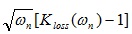 for a given set of frequency samples and solving the linear system e.g. by singular value decomposition method. For better accuracy, we can also normalize both parts of equation on
  . After solving equation for
  , unknown term
 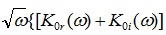 can be restored as imaginary part of (26).
Now, that we have approximation for real and imaginary parts  , we can find
 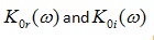 as
as
 (27)
(27)
Here, the functions 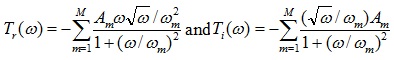 are fully defined by the chosen set of poles
  and found coefficients
  . The complex correction factor of interest becomes a combination of real/imaginary parts from (27).
Figure 9. Given loss factor (black), real and imaginary parts of the restored complex correction factor (red/blue) (a). Loss (red) and inductance correction factors (blue), restored by fit (b)
Unlike Figure 8, here we observe more stable behavior of the correction factors while ensuring sufficiently accurate fit of the loss factor.
VI. Cannonball-Huray Model
Building upon the work already done by Huray [3], the Cannonball model is used to determine the radius and base area parameters in the original Huray model. As opposed to the stacked sphere approximation using scanning electron microscopy (SEM) data, the Cannonball model determines the exact sphere radius and flat base area based solely on roughness parameters published in manufacturers’ data sheets.
Using the principle of stacking cannonballs, 14 uniform spheres, with radius (r), are stacked in a pyramidal structure, on a flat tile base, with an area Aflat, as illustrated in Figure 10
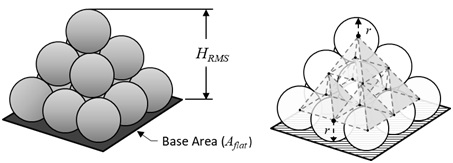
Figure 10. Cannonball model showing 9 spheres on the base row; 4 spheres in the middle row; and a single sphere on top. Five pyramid lattice structures join all 14 sphere centers as shown.
If we could peer inside the stack of spheres, and imagine 5 pyramids in a stacked lattice structure connecting the centers of all 14 spheres the radius can be easily determined by simple geometry and algebra.
Given the total height of the cannonball stack is equal to HRMS, then from method described in [11], determining the radius of a single sphere (r), from 10-point mean roughness (Rz) parameter from data sheet, can be further simplified and approximated by
 (CH-1)
And therefore the area of the flat tile base Aflat is
 (CH-2)
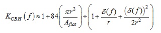
Since the Cannonball-Huray model assumes 14 equally sized spheres stacked in a cannonball stack, and the nodule treatment is applied to a perfectly flat surface, the original Huray model is simplified and thus the power loss correction factor, KCBH(f), can be determined by [11]:
 (CH-3)
where r is sphere radius in meters; δ (f) is skin depth, as a function of frequency, in meters, Aflat is an area of a single square flat tile base in sq. meters.
Case Study
To test the accuracy of the model, measured data, from a CMP-28 Channel Modeling Platform, courtesy of [9], [10] was used for model validation. The extracted de-embedded S-parameter data was computed from 2 inch and 8 inch single-ended stripline traces.
The printed circuit board (PCB) was fabricated with Isola [16] FR408HR 3313 dielectric and 1 oz. MLS Grade 3, controlled elongation reverse treated foil (RTF), from Oak-mitsui [17]. The data sheet and PCB design parameters are summarized in Table 2.
Dielectric constant, Dk dissipation factor, Df, and Rz are the values as reported in the respective manufactures’ data sheets. An oxide or micro-etch treatment is usually applied to the copper surfaces prior to final PCB lamination. The etch treatment creates a surface full of micro-voids which follows the underlying rough profile and allows the resin to squish in and fill the voids providing a good anchor. Because some of the copper is typically removed during the micro-etch treatment, the published roughness parameter of the matte side was reduced by nominal 50 μin (1.27 μm) for a new thickness of 4.445μm, used for matte side correction factor analysis.
Table 2. CMP-28 Test Board and Data Sheet Parameters
|
Parameter |
Value |
|---|---|
|
Dk Core/Prepreg @ fo |
3.68/3.62@1GHz |
|
Df Core/Prepreg @ fo |
0.0087/0.0089 @ 1GHz |
|
Rz Drum side |
3.048 μm |
|
Rz Before Micro-etch-Matte side |
5.715 μm |
|
Rz After 50 μin (1.27 μm) Micro-etch treatment -Matte side |
4.445 μm |
|
Trace Thickness, t |
1.25 mils (31.73 μm) |
|
Trace Etch Factor |
60 deg taper |
|
Trace Width, w |
11 mils (279.20 μm) |
|
Core thickness, H1 |
12 mils (304.60 μm) |
|
Prepreg thickness, H2 |
10.6 mils (269.00 μm) |
|
De-embedded trace length |
6.00 in (15.24 cm) |
In [12], the authors observed an increase in phase delay proportional to roughness profile and dielectric material thickness. In [13] it was shown that the increased phase delay can be partly attributed to increased capacitance due to surface roughness. Because laminate suppliers’ data sheets typically report Dk as the value measured in a production environment, it does not guarantee the values are correct for design applications. In most cases the value published is lower that what is finally measured after the PCB has been fabricated.
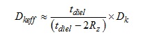
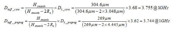
If the roughness of copper foil and dielectric constant from manufacturers’ data sheets are known, then the increase in effective dielectric constant (Dkeff) can be approximated by [13]:
 (CH-4)
where tdiel is the dielectric material thickness, Rz is the 10-point mean roughness, and Dk is the dielectric constant for as published in respective manufacturers’ data sheets.
From Table 2 and by applying (CH-4), Dkeff of core and prepreg due to roughness were determined as
A modified version of Mentor HyperLynx [14] was used to include causal/non-causal conductor models and Cannonball-Huray correction factors for matte and drum sides of the foil based on (CH-3). Corrected Dkeff for core and prepreg, based on (CH-4), were used while Df for core and prepreg remained unchanged from Table 2.
Keysight ADS [15] was used for simulation analysis and comparison to measured data. Frequency domain results are presented in Figure 11. The left graph shows measured insertion loss of a de-embedded 6 inch stripline trace vs causal and non-causal models. As can be seen, there is virtually no difference between causal and non-causal model simulations.
The right graph of Figure 11 shows measured phase delay vs causal and non-causal models. The non-causal model is consistent with phase delay compensation results published in [13]. But when the causal version of conductor roughness model was applied we observe that simulated phase delay matches measured phase delay almost exactly. This is remarkable, considering there was no additional tuning or curve of fitting parameters from manufacturers’ data sheet values.
Figure 12 shows simulated vs measured results. Time delay transmission (TDT) impulse response is shown on the left graph while time domain reflected (TDR) impedance is shown on right graph. As can be seen, there is excellent correlation between causal models and measured data for both graphs. Also worth noting, the causal model has higher characteristic impedance and is a better fit to measured results compared to non-causal model as expected.
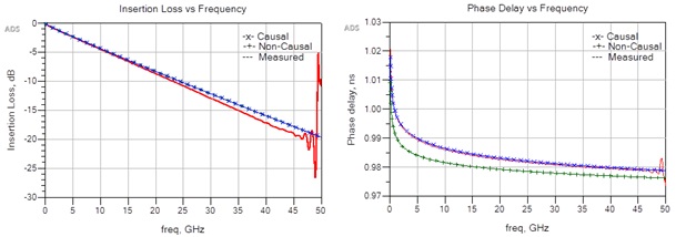
Figure 11. Causal / non-causal vs measured insertion loss (IL) (left) and phase delay (right).
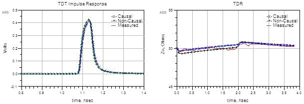
Figure 12. Causal / non-causal vs measured time domain transmission (TDT) impulse response (left) and time domain reflected (TDR) response (right).
Conclusion
In this paper, we presented a causal version of the roughness correction factor associated with certain loss models. Although the Hammerstad and Cannonball-Huray models have been considered in detail, the method described in this work also applies to other models, given by formulas or tables.
We considered the impact created by causality of metal roughness on the characteristics of transmission lines. The effect it makes on insertion loss, phase delay, and characteristic impedance was described analytically as functions of PUL parameters. These formula estimates show perfect agreement with simulated results.
We also demonstrated that phase delay and characteristic impedance considerably increased, compared to the case of using a non-causal, real-value correction multiplier. Simulated results appear in a perfect agreement with measured characteristics of the example case study.
In the end, we note that causal and non-causal models of metal roughness are not just two versions of the same model. Causal models could be wrong in many ways, but at least they have a potential to correctly describe the relation between the current density and the electric field on metal’s surface, which is a causal function. A non-causal model, on the other hand, is always wrong, and it’s only a question of how large the error it brings into simulation.
Download the Link to Appendix A and Appendix B for more detailed equations
This article is an edited version of a DesignCon 2018 Best Paper Award winner.
Download the full paper here
References
[1] S. Hall, S. Pytel, P. Huray et al. “Multigigahertz causal transmission line modeling methodology using a 3-D hemispherical surface roughness approach,” IEEE Trans. on Microwave Theory and Techniques, v.55, No.12, 2007
[2] S. Hall, H. Heck, “Advanced signal integrity for high speed digital designs,” John Willey & Sons Inc., Hoboken, NJ, 2009.
[3] P. Huray, “The foundations of signal integrity,” John Willey & Sons Inc., Hoboken, NJ, 2009.
[4] E. Bogatin, D. DeGroot, P. Huray, and Y. Shlepnev, “Which one is better? Comparing options to describe frequency dependent losses,” DesignCon 2013.
[5] Appendix E. “Causal relationship between skin effect resistance and internal inductance for rough conductors,” – in [2].
[6] E. Bracken, “A causal Huray model for surface roughness”, DesignCon 2012.
[7] A. Djordjevic, R. Biljie, V. Likar-Smiljanic, T. Sarkar, “Wideband frequency domain characterization of FR-4 and time domain causality”, IEEE Trans. on EMC, vol.43, No.4, 2001.
[8] Y. Shlepnev, “Modeling frequency-dependent dielectric loss and dispersion for multigigabit data channels”, Simbeor Application Note 2008.
[9] Simberian Inc., 3030 S Torrey Pines Dr. Las Vegas, NV 89146, USA. URL: http://www.simberian.com/
[10] Wild River Technology LLC 8311 SW Charlotte Drive Beaverton, OR 97007. URL: https://wildrivertech.com/
[11] B. Simonovich, "Practical model of conductor surface roughness using cubic close-packing of equal spheres", Signal Integrity Journal, 2016
[12] A. F. Horn, J. W. Reynolds and J. C. Rautio, "Conductor profile effects on the propagation constant of microstrip transmission lines," Microwave Symposium Digest (MTT), 2010 IEEE MTT-S International, Anaheim, CA, 2010, pp. 1-1.doi: 10.1109/MWSYM.2010.5517477
[13] B. Simonovich, "A practical method to model effective permittivity and phase delay due to conductor surface roughness", DesignCon 2017
[14] Mentor Hyperlynx [computer software] URL: https://www.mentor.com/pcb/hyperlynx/
[15] Keysight Advanced Design System (ADS) [computer software], (Version 2016). URL: http://www.keysight.com/en/pc-1297113/advanced-design-system-ads?cc=US&lc=eng
[16] Isola Group S.a.r.l., 3100 West Ray Road, Suite 301, Chandler, AZ 85226. URL: http://www.isola-group.com/
[17] Oak-mitsui 80 First St, Hoosick Falls, NY, 12090. URL: http://www.oakmitsui.com/pages/company/company.asp
Author(s) Biography
Dr. Vladimir Dmitriev-Zdorov is a principal engineer at Mentor Graphics Corporation. He has developed a number of advanced models and novel simulation methods used in the company’s products. His current work includes development of efficient methods of circuit/system simulation in the time and frequency domains, transformation and analysis of multi-port systems, and statistical and time-domain analysis of SERDES links. He received Ph.D. and D.Sc. degrees (1986, 1998) based on his work on circuit and system simulation methods. The results have been published in numerous papers and conference proceedings.
Bert Simonovich graduated from Mohawk College of Applied Arts and Technology, Hamilton, Ontario Canada, as an Electronic Engineering Technologist. Over a 32-year career, working at Bell Northern Research/Nortel, in Ottawa, Canada, he helped pioneer several advanced technology solutions into products. He has held a variety of engineering, research and development positions, eventually specializing in high-speed signal integrity and backplane architectures. After leaving Nortel in 2009, he founded Lamsim Enterprises Inc., where he continues to provide innovative signal integrity and backplane solutions as a consultant. He has also authored and coauthored several publications; posted on his web site at www.lamsimenterprises.com. His current research interests include: high-speed signal integrity, modeling and characterization of high-speed serial link architectures.
Dr. Igor Kochikov received his PhD degree in computational mathematics from Moscow State University in 1985. Since 1998 with Mentor Graphics, focusing on PCB and interconnect electromagnetic modeling, providing software architecture definition and development of the fast and reliable simulation methods in signal integrity and power integrity applications. He has also been involved in computer-aided research in various fields of physics and authored several books and numerous papers in physical chemistry, optics, spectroscopy and molecular structural analysis.