
In Part 1 of this article series, we explored the significance and impact of Dk and DF on key performance attributes. In this article, we move on to talk about the impact that conductor roughness has on performance attributes as well as a third major signal integrity performance attribute—namely, skew.
Roughness and Skew
Two key attributes that deserve their own discussion are roughness and skew. Roughness warrants special discussion, as it is a key contributor to insertion loss performance. Skew also warrants special discussion, as it is a major signal integrity performance characteristic (in addition to impedance and loss) that can make or break a design and cause field failures.
Conductor Roughness
In the early days of the industry, copper foil had a high roughness profile, designed to ensure strong adhesion with the dielectric materials. These profiles were relatively fast and easy to process and were used through most applications. As the industry went up the speed curve, newer lower loss materials, such as discussed in Part 1 of this series, emerged. However, the gains from these lower loss materials were limited because the contribution to the loss from the high copper roughness was still very high. Thus, as signal integrity considerations became more important, lower profile copper became necessary to meet the ever-shrinking loss budgets.
Conductor roughness profiles are key drivers of conductor loss, and, in turn, insertion loss behavior of transmission lines. They also influence the impedance through their impact on the imaginary component of the inductance, so it is important to understand their role in the PCB process.
While PCB fabricators may still like higher profile copper for the strong adhesion and high peel strength, copper roughness profiles down to Rz values of less than 1 µm are available now. However, it has become increasingly critical to look not only at the copper foil, but also the oxide when evaluating signal integrity behavior and assessing insertion loss.
Copper foils for high-speed and high-frequency applications (typically with Rz values below 3 µm) are typically provided with one side having a relatively low roughness profile and the other side having a relatively high roughness profile. When the boards are built, the lower roughness profile side comes bonded to the core (or is similarly bonded to a prepreg during sequential lamination in HDI designs), whereas the higher roughness profile side is treated with an oxide. That oxide effectively becomes the surface that adheres to the dielectric and also replaces the roughness profile of the original untreated copper.
While just looking at the low roughness profile of the copper foil can often allow you to simulate a reasonable estimate of your insertion loss, in order to truly extract high accuracy, all sides of the copper foil must be considered. As such, simulations should be conducted with multi-sided roughness, when possible, such as shown in Figure 1. Figure 1 shows the Hammerstad model so as to not look busy with multiple parameters, but this could also be applied to Huray or Causal-Huray models. A discussion on these different roughness models is outside the scope of this article, but, suffice to say, a roughness model helps allow you to capture the roughness profile and its impact on transmission line behavior.
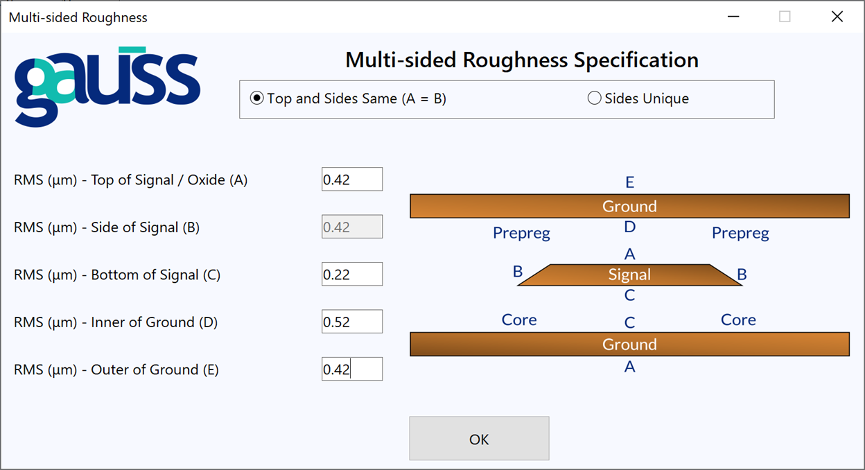 Figure 1. Multi-sided roughness specified for a stripline using Hammerstad model.
What is Skew and Why Does it Occur?
To start, I wanted to simply define what skew is and how it emerges in PCBs. Skew (sometimes called “clock skew” or “timing skew”) is the phenomenon of two signals arriving at their destinations at different intervals. Intra-pair skew is primarily of concern when dealing with signals that are supposed to be synchronous, such as when dealing with differential pairs.
Given that the typical dielectric materials available in the market are built on woven glass reinforcements, a trace may run over, through its length, any combination of glass fiber, pure resin, and knuckles where glass fiber is woven over other glass fiber. Figure 2 below illustrates this phenomenon by showing three examples of trace location for the same differential pair. The dielectric constants of the resin and glass have a large mismatch, which means that two parallel traces, such as those in a differential pair, may have very different effective dielectric constants, which, in turn result in very different times of flight, causing skew. This is referred to as fiber weave skew or the fiber weave effect.
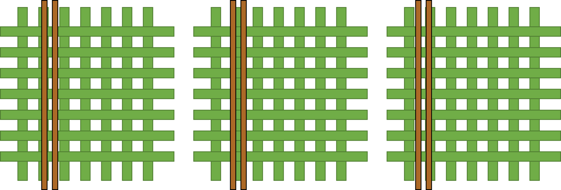 Figure 2. Woven glass and resin. Drivers of fiber weave skew.
The industry has long been concerned with approaches to reduce skew—mechanical spreading of glass weaves, use of low Dk glass, multiple plies in a dielectric opening, routing over the weft direction (to take advantage of meander). The problem is that, like most of the other aspects we’ve looked at here, there are numerous parameters that will affect the skew—such as the lines and spacings, the resin system, itself—and this makes blindly following some kind of rule unfeasible. This brings us back to the same possible solution of either extensive testing or specific simulation. Figure 3 and Figure 4 below shows two extreme examples of a very low skew and a very high skew on the same layer of the same stackup. As a note, the distributions shown are sampling distributions with 20,000 samples of different placements of the differential pair relative to the weave (while maintaining the specified line-width and spacing).
 Figure 3. A reference differential pair showing high skew.
 Figure 4. A differential pair with low skew on the same layer and in the same stackup as the one shown in Figure 3, but with different line
-width and spacing.
Another often-proposed solution to skew is the rotation of a panel by, say, 3° or 10°. While such rotation can often greatly reduce or even eliminate the skew, yields are reduced, as much less of a panel’s footprint is accessible for cutting out a circuit. Additionally, this introduces resonance1, wherein the major concern would be a sudden, very large rise in insertion loss, at frequencies that may fall within the operating windows of on-board frequencies. Figure 5 below shows an example of resonance caused by a 3° rotation, which would occur at frequencies of around 12.07 GHz and 12.31 GHz.
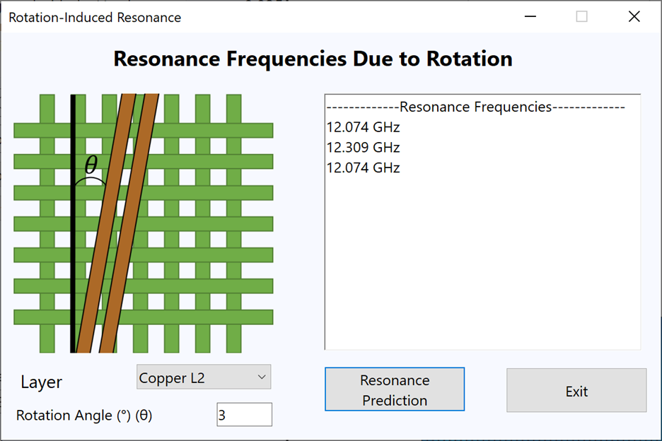 Figure 5. Resonance from rotation.
The primary goal of simulation and/or testing is to determine the window(s) within which one can attain the desired behavior. However, with the problem of skew, the current highest frequency, highest data rate applications have no material solution, as the skew budgets for 112 Gb/s or 224 Gb/s per channel are so small that, ostensibly, a no-skew solution is required. Many product implementations are currently using flyover cables and other board bypassing solutions as a stopgap, but the costs associated with this are high and there are key limitations, especially with regard to footprint (for example, you can’t use flyover cables in a mobile phone).
But, as they say, necessity is the mother of all invention and there are promising no-skew technologies that some folks in the industry are working on, some of which may be commercialized sooner rather than later.
Summary
Beyond Dk and DF of a dielectric material, copper foil and oxide roughness are also major drivers of insertion loss behavior. As discussed in Part 1 of this article series, the first crucial step to efficacious design and development is understanding how the dielectric material attributes are to be carefully considered when assessing impedance and insertion loss performance. However, it is also crucial to consider the roughness attributes discussed in this article in this assessment. Beyond impedance and loss, skew is a signal integrity concern of ever-increasing importance; understanding the complexities that cause the problem, as well as the ways to test, simulate, and mitigate it will serve one well in any high-speed design endeavor.
You can read Part 1 of this article to learn more about Dk and DF here.
Footnotes
1For anyone interested in learning more about why such rotation could induce resonance, this emerges from the periodicity of the fiber weave. Such behavior is characterized through Floquet-Bloch theory, which can be best understood through study of an introductory solid-state physics, wave-physics, or phonon physics textbook. Either Collin (Field Theory on Guided Waves by Robert E. Collin) or Kittel (Introduction to Solid State Physics by Charles Kittel) would be good starting points for a deeper dive into such periodic structures and behavior.