
Editor’s Note: Microwave Journal asked some of the leading electromagnetic compatibility (EMC)/electromagnetic interference (EMI) electronic design automation (EDA) software suppliers to provide a description of their features for EMC/EMI applications and unique solving capabilities for these markets.
Altair/FEKO
Stellenbosch, South Africa
FEKO assists original equipment manufacturers (OEM) and their suppliers across many industries to solve EMC problems related to design, analysis and validation. By using software applications such as FEKO, the number of prototypes and tests are reduced, which changes the development process from measurement-driven to simulation-driven. Key applications where FEKO is being used on EMC/EMI include emissions, immunity, lightning effects, high intensity radiated fields (HIRF), electromagnetic pulses (EMP), shielding, radiation hazard and antenna coupling, among others.
EMC Simulation
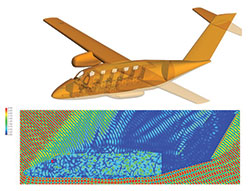
Figure 1 Aircraft and magnetic field strength at 1 GHz computed by FEKO.
Antenna coupling in platforms is one of the sweet spots of FEKO (see Figure 1). This aircraft geometry is part of the Computational Electromagnetics for EMC (CEMEMC) workshop and corresponds to a morphed version of EV55 (Intellectual Property of EVEKTOR, spol. s r.o. and the HIRF SE Consortium, HIRF-SE FP7 EU project). Depending on the problem and its electrical size and complexity, users just need to select one of the solvers in FEKO. One way to easily calculate antenna coupling in FEKO is through S-parameters, where users can see the effect of changing antenna loads without re-running the solver, easily visualize results for a large number of ports and plot a co-site interference matrix to visually identify and analyze critical couplings. In addition to this, model decomposition in FEKO works with equivalent antenna and EMC sources to reduce computational requirements.
EMI Design Challenges
There are multiple key use cases related to EMI being solved with FEKO. For example, coupling of radiated fields from cable harnesses to windscreen antennas (and to other types of antennas) in a vehicle, also related to CISPR-25 EMC standard (CISPR is the International Special Committee on Radio Interference or Comité International Spécial des Perturbations Radioélectriques) that sets industry test standards. There can be noisy signals propagating through different cables in the car and the radiation from such cables is coupled into different antennas, adding noise, thus reducing the performance of systems like analog or digital radio. To address this, FEKO includes a complete integrated cable modeling tool that permits the analysis of the radiation (and irradiation) of cables. This tool, together with a windscreen antenna method specifically designed to model real windscreen antennas, permits one to analyze and find solutions related to these cases (see Figure 2). In Figure 2b, fields at two points are simulated at 10 m, and for each point the vertical and horizontal polarizations are calculated.
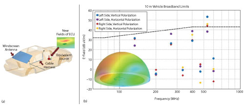
Figure 2 Car model with windscreen antenna, cable harness and equivalent source for the engine control unit (ECU) (a) and simulated electric near fields including measurement setup (b).
Unique Features
FEKO is easy to use and has a comprehensive, accurate, reliable and fully parallelized set of solvers with true hybridization, including Method of Moments (MoM), Multilevel Fast Multipole Method (MLFMM), Finite Element Method (FEM), Finite Difference Time Domain (FDTD), Physical Optics/Large Element-Physical Optics (PO/LE-PO), Ray-Launching Geometrical Optics (RL-GO) and Uniform Theory of Diffraction (UTD). These solvers are widely used to solve antenna design and placement, EMC, radar cross-section (RCS), bio-electromagnetics, radomes and RF devices problems, among others. Depending on the electrical size and complexity of the problem, one solver or another just needs to be used. FEKO’s integrated cable modelling tool addresses EMC problems involving complex cables. Two special methods in FEKO for cables are Multi-Conductor Transmission Line (MTL) and the combined MoM/MTL, which is used for real problems where ground planes below the cables are not continuous. FEKO, as part of Altair HyperWorks Computer Aided Engineering (CAE) platform, brings a set of additional and differential capabilities that can be leveraged at no extra cost due to Altair’s unique licensing system. Very complex Computer Aided Design (CAD) models can be cleaned-up and meshed in less time (including automation) thanks to HyperMesh, a leading finite element analysis pre-processor. With HyperStudy, FEKO users can perform design of experiments to further optimize designs, including other physics analysis, and with activate electrical circuits, like DC/DC converters, can be analyzed and designed.
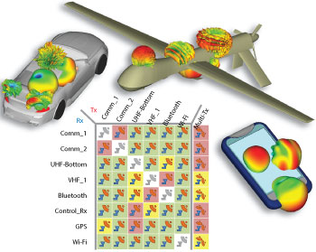
Figure 3 Examples of multi-radio and radio-digital systems that can be analyzed with ANSYS EMIT.
ANSYS
Canonsburg, Pa.
The problem of RF interference between co-located platform integrated radios can be difficult to manage. With continued integration into the IoT infrastructure, modern commercial electronic devices are becoming ever more complex and feature rich with increasing wireless capability. This dense wireless capability has resulted in an exponential growth of the radio frequency interference (RFI) problem throughout the electronics industry. Examples of radio environments are a single structure such as an airplane, satellite, wireless electronic device or multiple radios in a more dispersed environment, such as many wireless devices within an office setting or at outdoor cell communications sites. These multiple, multi-band RF systems need to coexist peacefully and “play well” together and not degrade the performance of the other systems in the environment. And the problem of interference is not limited to explicit radio channels. Electronic devices are composed of both RF and digital signals and components which can share a common ground plane or reference. The digital signals alone, although typically operating at clock frequencies below the radio frequencies, can contain harmonics that interfere with the radio channels through their common reference geometry. This latter, RF-digital interference is commonly referred to as de-sense, and is one of the more difficult design challenges in wireless electronic devices since it requires a complete system understanding to predict and/or detect (see Figure 3).
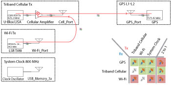
Figure 4 Interaction diagram and scenario matrix from EMIT, used to reconstruct interference paths and identify root causes for EMI.
ANSYS EMIT for EMI Analysis
ANSYS EMIT is an industry leading software for the simulation of RFI in complex environments. EMIT works together with ANSYS HFSS and HFSS SBR+, formerly Delcross Savant, to combine RF system interference analysis with best-in-class electromagnetic simulation for modeling installed antenna-to-antenna and radio-to-radio coupling. This solution reliably predicts the effects of RFI in multi-antenna environments with multiple transmitters and receivers. EMIT’s analysis engine computes important RF interactions, including nonlinear system component effects. Diagnosing RFI in complex environments is notoriously difficult and expensive to perform in a testing environment. To address this challenge, EMIT provides a dynamically linked result view to aid in the identification of the root-cause of interference via graphical signal trace-back and diagnostic summaries. These summaries show the origin and paths of transmit-to-receiver interfering signals (see Figure 4).
With the cause of interference uncovered, EMIT enables rapid evaluation of various RFI mitigation measures to arrive at an optimum solution. Including accurate physical effects associated with electromagnetic coupling will improve the fidelity and reliability of the RF system simulation. An HFSS/EMIT datalink allows the model for RFI analysis to be created in EMIT directly from the physical 3D model of the installed antennas in HFSS, providing a seamless end-to-end workflow for a complete RFI solution of systems and environments ranging from large platform co-site interference to receiver de-sense in compact electronic devices.
ANSYS EMIT in the ANSYS RF Option provides a software framework for managing system performance data including a library of RF systems, a computational engine for simulating RFI effects in complex multi-system environments, a dynamic analysis tool for rapid automatic identification of the root-cause of RFI problems and allows engineers to quickly evaluate different “what-if” analyses to resolve EMI issues.

Figure 5 Surface currents on an aircraft during a lightning strike.
Computer Simulation Technology (CST)
Darmstadt, Germany
EMC Challenges
CST EMC STUDIO is an EM simulation tool used by industry leaders to analyze and optimize products for performance and compliance with EMC norms. The CST “Complete Technology” approach means that CST EMC STUDIO includes a range of solvers for many different scenarios, from general purpose time and frequency domain solvers to specialized solvers for cables and printed electronics. These solvers are all included in one interface, allowing for a uniquely integrated workflow.
Both CAD data and printed circuit board (PCB) layouts from EDA tools can be imported into CST EMC STUDIO. Specialized PCB simulation tools can quickly calculate signal integrity and power integrity (SI/PI) and identify violations of EMC design rules, while the general purpose 3D solvers can simulate radiated and conducted emissions/susceptibility in detail. Fields and currents on the 3D structure, including the attached circuits, can be visualized to help engineers identify coupling paths.
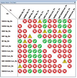
Figure 6 The Interference Task shows which combinations of RF systems can lead to co-site interference.
EMI Challenges
Immunity to emissions and environmental electromagnetic effects (E3) such as lightning is an important application (see Figure 5). The Transmission Line Matrix (TLM) Solver is especially well suited to these applications, and can simulate very large structures effectively. It supports octree meshing and compact models of seams, vents, composite materials and other relevant features, which can further accelerate simulations while maintaining accuracy, and also offers bi-directional coupling to CST CABLE STUDIO for simulating how fields couple into and propagate through cables and cable harnesses.
Another major application of CST EMC STUDIO is antenna coupling. In a typical antenna-to-antenna scenario, the antennas may be installed on extremely large platforms such as aircraft, ships or buildings, but the coupling itself can depend on fine details such as the exact design of the antenna or the seams, vents and cables in the platform. CST EMC STUDIO supports a hybrid approach where the antennas can be simulated in detail with a suitable solver such as the Time Domain Solver, and then used as field source for a coupling simulation with a different solver such as the Integral Equation Solver, TLM Solver or Asymptotic Solver. Combining solvers in this way gives engineers the best of both and can significantly speed up simulation times.
As well as calculating the coupling between subsystems, such as antennas on a platform or channels on a PCB, a co-site interference analysis also involves taking into account the frequency spectra of each subsystem. The Interference Task, new in CST EMC STUDIO 2017, offers a straightforward approach for investigating potential EMI issues using coupling data from simulations combined with information about each Rx/Tx system (see Figure 6). Using this, the Interference Task produces a violation matrix highlighting combinations that could potentially lead to EMI issues. This is a very effective way to identify EMI problems and test mitigation approaches on a virtual prototype.
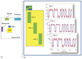
Figure 7 Example of a mobile device layout (a) and self-jamming vs. locations of the digital interface on the PCB (b).
Keysight Technologies
Santa Rosa, Calif.
EMI and EMC are not new issues for system engineers. However, with increasing data rates in computers, networks, storage and mobile devices, design engineers are more challenged to deal with not only the traditional emission issues, but also coupling issues with nearby circuit and system components. Overcoming these challenges using appropriate design tools is essential to successful system design.
RF De-sense or RFI Issues
One of the issues designers face when it comes to EMC and EMI is interference between subsystems and antennas. It is an especially severe problem in mobile devices, where designs are squeezed into very small areas. The interference can cause degradation in receiver sensitivity, also known as “RF de-sense” or “RFI” issues. For example, high-speed application processors, memories, camera modules, DC-DC power converters and high-speed interconnects, like USB 3.1 Type C, may cause “self-jamming” issues with RF circuits that include multi-band antennas (see Figure 7).
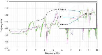
Figure 8 Cellular, WLAN and Bluetooth antenna coupling in a mobile phone.
Integrated Circuit and EM Simulation is Necessary
Diagnosing RF de-sense and self-jamming issues presents a real challenge for today’s designers. They must model EM field interactions within devices using EM solvers and be able to handle digital waveforms from circuit- and system-level design tools. For these tasks, a design environment that integrates both circuits and EM is a must. Keysight’s Advanced Design System (ADS) and EMPro provide a uniquely integrated software design platform that offers a solution.
Antenna-to-Antenna Coupling Issues
With many antennas crammed into a very small piece of real estate, the coupling between antennas can become quite problematic (see Figure 8). This type of coupling may or may not be as significant if designers use different frequency bands. Designers can also employ the use of bandpass or band-rejection filters, which may reduce unwanted energy coupling. Careful design of the whole device is required, including co-design of the on-board antennas with the ground plane.
Since antenna-to-antenna coupling is mostly a near field problem, it can be accurately handled with traditional EM simulation technologies such FEM, MoM or FDTD engines. The coupling problem may be mitigated by adjusting the position of the antennas and/or tweaking the antenna performance, such as gain versus frequency or radiation patterns.
With Keysight design tools, designers can simulate the radiated emissions of electronic circuits and components, determine whether these emissions are within levels specified by common standards, such as FCC Part 15, CISPR 22 and MIL-STD-461F, and whether they are compliant—all before hardware has been developed.
In addition to verifying EMI compliances, it is critical to have the correct noise waveform injected for an accurate calculation of emission level. Keysight tools offer designers access to many different waveforms, whether standard waveforms, user-defined or measured waveforms.
Integration is Key
As data rates continue to increase, system designers will likely face even greater EMI and EMC design challenges. Using the right design tools that offer integrated circuit and EM simulation are essential. Keysight’s design tools not only offer that level of integration, but are designed to handle a range of design issues, making them ideal for helping system engineers overcome the EMC and EMI design challenges they face today and in the future.
NI AWR
El Segundo, Calif.
Addressing EMC/EMI performance is an integral part of product development, especially when electronics are densely packed, causing high-frequency signals and fast transients to give rise to either radiated or conducted (transmission) emissions with the potential to adversely affect each other. NI AWR Design Environment, an open design platform for high-frequency circuit and system product development, addresses these concerns with integrated design tools that incorporate planar and arbitrary 3D EM analysis directly within circuit- and system-level design and simulation. The analysis capabilities offered through integrated circuit, system and EM co-simulation are illustrated with the following two examples in which the capabilities in NI AWR software were leveraged to overcome several EMC/EMI design challenges.
Figure 9 EMC radiation noise analysis model.
Mitsubishi Example
Designers at the Mitsubishi Electric Corporation used NI AWR Design Environment to tackle their EMC/EMI design challenges and improve the sound quality of the company’s DIATONE car audio system. The design team used Microwave Office circuit design software and AXIEM planar EM analysis software to perform a rigorous EMC noise analysis of the navigation system’s circuit board design, including identification of the noise source through analysis of the transmission path and the radiation noise.
The designers considered the overall system, which included an emission source (emitter) and susceptible receptors within a given environment. EMI comes from EM waves that are generated by the integrated circuit. Modeling the high-frequency noise comprised three basic components: noise source, transmission path and radiation end, as shown in Figure 9.
In this model, the audio board was designed using a two-board configuration of a power supply board and a main board containing a microcontroller, digital signal processor and digital-to-analog converter. The designers developed an accurate model of the noise source as verified through measurements in a test system. This model was then used in conjunction with EM simulations of possible board geometries to investigate how to mitigate EM problems (see Figure 10). The improvement in anti-noise measures combined with a significant reduction in the number of trials resulted in a dramatic reduction in overall trial cost while still maintaining sound quality.
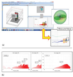
Figure 10 EMC radiation noise analysis model (a) and elimination of resonances after anti-noise measures were implemented in the design (b).
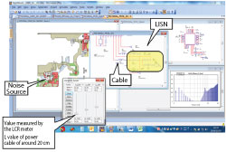
Figure 11 Integration of circuit analysis with EM modeling speeds problem identification and resolution.
The tight coupling of Microwave Office and AXIEM accelerated the design process tremendously. EMC noise analysis of the transmission noise components revealed a return path that resulted in a degradation of the audio system sound quality. Hot spots were quickly identified with AXIEM’s current view; changes to components could then be quickly implemented in Microwave Office, which in turn coupled back into AXIEM results, as shown in Figure 11. Through EMC noise analysis, the trial cost was reduced by at least 60 percent, the parts cost was reduced by at least 30 percent, the labor cost was reduced by at least 60 percent and the utility cost was reduced by at least 50 percent.

Figure 12 Circuit model of notched-band filter.
RF Microtech Example
Another EMI/EMC design challenge was successfully addressed by RF Microtech using NI AWR Design Environment in the design of a very large and complex ultra-wideband (UWB) filter for use in preventing mobile service bands from interfering with a critical security control base station at Expo Milano 2015. This type of problem differs from the first example, in that the designers were asked to develop a high-performance filter from interfering signals with known characteristics. The challenge was to develop this filter in less than a month.
RF Microtech was challenged to provide a validated full-wave EM simulation of a two-port UWB filter that could reject all five mobile service bands with greater than 35 dB. The validated EM simulation had to be delivered within two weeks and the complete deployable device by the time the expo opened. The design team used Microwave Office to develop a circuit model of five independent notched-band filters (NBF) cascaded along a transmission line (see Figure 12).
Each independent filter was designed as a fourth or fifth order NBF, composed of several cascaded stages of N shunt resonators. The individual filter specifications called for resonators with high unloaded Qs (>1000) and no spurious modes under 6 GHz. After identifying the optimum filter geometries, the transmission line and filter sections were verified in ANSYS HFSS full-wave EM analysis tool.
These two use cases have illustrated how EMC/EMI performance issues were overcome with the use of NI AWR Design Environment integrated circuit and EM design tools that enabled both design teams to dramatically cut design cycles and costs and deliver high quality solutions on time.