
Typically, high-frequency VNAs measure interconnects and other RF devices on test fixtures. Test fixtures are something that signal integrity (SI) engineers need, but do not want. They are expensive, difficult to design, and cloud the performance of the device under test (DUT). De-embedding makes the murky waters between the SI engineer and the DUT clear by removing the fixture from the measurement.
De-embedding isolates the DUT using an algorithm that mathematically removes the test fixture from the measurement. In addition to measuring the DUT on the test fixture, de-embedding requires extra measurements of devices called standards. The de-embedding algorithm uses the standards to calculate a model of the test fixture called an error box. The error box is in the form of a matrix, and it is removed from the measurement with matrix algebra.

An error box is often referred to as a “fixture model” by measurement equipment vendors. The phrase “error box” is the language used in academic journals and text books, and the phrase “fixture model” is jargon used in industry. Further, the word “box” in “error box” comes from its shape in the signal flow graph. There is also something called an “error model” which does not look like a box. The phrase “error model” has a number as a prefix. Internal VNA short-open-load-thru (SOLT) calibration adjustments use a 12-term error model to remove artifacts between the VNA sampler and the port. The term “error box” in this article is also a 4-term error model.
If you are an experienced individual looking to learn more about the technical side of de-embedding, feel free to jump to “Styles of De-Embedding” section.
When to De-embed and Why
Two primary reasons to de-embed are:
- To directly compare measurement to simulation
- To analyze an isolated component
In interconnect and high-speed serial component design, 3D simulations predict component performance (see Figure 1). These predictions are faster and more cost-effective than prototyping concepts. However, nothing is like the real thing. There is a SI saying that goes “Everyone believes a measurement except the one who took it, and no one trusts a simulation besides the one who made it.” Therefore, all interested parties want to see just how close the measurement and simulation are.
After a component (DUT) has been designed and its performance validated using simulation tools, test fixtures are designed and fabricated, and the DUT is placed upon them (see Figure 2). The entire setup is taken into the lab where every accessible port is measured. The lab creates a report comparing the measured and simulated S-parameters, and “viola!” the measurement looks nothing like the simulation (see Figure 3). Woe is the SI engineer!
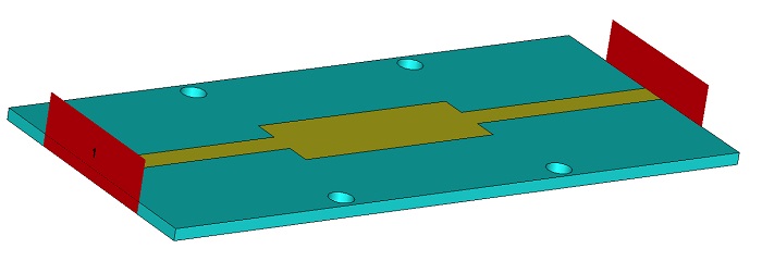
Figure 1: Simulated serial resonator
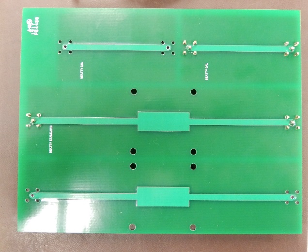
Figure 2: Fabricated serial resonator and 2x thru calibration structure
Note: There are two 2x thrus and two serial resonators on this board because adding a second set was free.
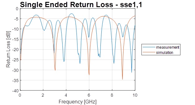
Figure 3: Return Loss of the measured and simulated structure
This is where de-embedding comes in. An extra trace, called a 2x thru, is usually available on test fixtures. Using a measurement of a 2x thru, the error boxes are calculated, and the fixture is de-embedded. A new report is made with the de-embedded S-parameters, and the simulation and measurement look similar (see Figure 4). The bottom line is that component simulations cannot be properly compared to measurements without de-embedding the test fixture.
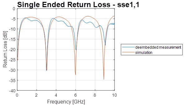
Figure 4: Return Loss of the de-embedded measurement and simulated structure
In another scenario, high-speed serial channel designers need to pick components. The performance of these components sometimes comes in the form of datasheets or S-parameters. A good SI engineer will validate any information coming from a vendor, because as you know, everyone trusts a measurement. To give the customer a way to measure the component, vendors typically provide RF components to customers on evaluation kits. These evaluations kits are simply the component properly mounted to a test fixture. It is important to isolate the component from the test fixture to make sure it is viewed in the best light possible, because false failures lead to unnecessary searches for new solutions. De-embedding isolates the component for proper and fair analysis.
Problems with De-embedding
It might sound easy, but de-embedding is difficult. Some find the techniques for de-embedding difficult to understand and implement. In addition, the fixture design can limit the quality of the DUT’s isolated S-parameters. To help SI engineers and lab technicians alike understand the techniques, the following sections present SOL, TRL, and 2x Thru algorithms and how to implement them.
De-embedding algorithms are mathematically perfect. Simulations show how de-embedding removes complex test fixtures without error. However, in the real world, de-embedding without error is not achievable. Two primary sources of error in de-embedding are poor measurements, and standards that are different from the DUT fixture.
Poor measurements come in two flavors: invalid reference planes and high noise floors. Invalid reference planes are caused by improper fixture design or improper use of torque wrenches. Improper fixture design is an easy one to prevent; just follow the rules in the next sections. Improper use of the torque wrench is more difficult. When force is applied at a certain location on the wrench, the torque wrench is calibrated to release after the twisting force in one direction is exceeded. When using the torque wrench properly, the male pin of the coaxial connector will be inserted at a controlled depth, and every measurement’s reference plane will be the same. In practice, technicians and engineers like to grab the wrench near its head, and this leads to inconsistent pin depth and reference plane.
High noise floors are easy to identify because the S-parameters resemble a jagged horizontal line at the noise floor. The level of this line is also called the dynamic range. The dynamic range of devices that capture S-parameters from the time domain are between -20 dB and -40 dB. VNAs are capable of much better: as low as -120 dB. Using more averages can improve the dynamic range of time-domain devices. However in practice, the dynamic range limit of time-domain devices is near -50 dB. By contrast, the VNA’s dynamic range is associated with its IF bandwidth; the lower the IF bandwidth, the better the dynamic range. 1 KHz IF bandwidth is a nice compromise between accuracy and speed.
Test fixture standards used to isolate DUTs are either transmission lines or transmission lines with a load. The standard’s transmission lines are designed with the same geometry as the test fixture’s traces. However, the impedance is always different between the two. Typically, a ±5% manufacturing tolerance is placed on the impedance. Lower tolerances are achievable through higher scrap rates for the boards, but this leads to extra cost. Thus, in practice 5% is usually the best that one can expect for a reasonable price.
Engineers design single-ended transmission lines to match the impedance of the test equipment which is typically 50 ohms. At worst case, which happens quite often in practice, the test fixture will be 5% high and the standard will be 5% low. This leads to a five-ohm difference between the standard and the fixture that is supposed to be removed. In this scenario, a “ripple” is seen in the reflected S-parameters (see Figure 5). To minimize impedance mismatch between fixture and standard, use ¼ or ½ oz copper and use stripline transmission lines. Using thin copper allows the copper etch solution to quickly remove unwanted copper, and minimizes the impedance variation associated with the etch factor. Using stripline traces also removes the ambiguity associated with plating and solder mask.
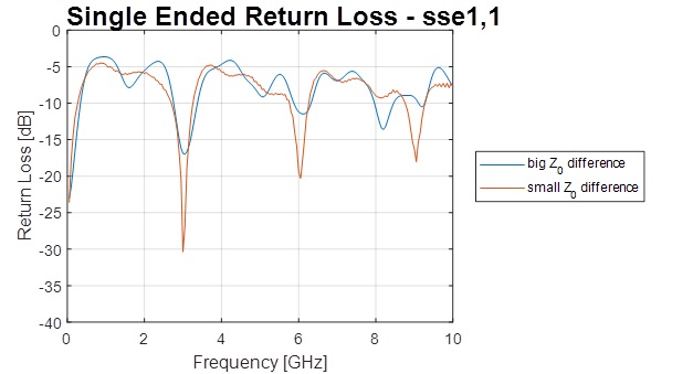
Figure 5: Return loss of a DUT. Considering the blue trace, the standard’s impedance is 10% higher than the DUT’s fixture impedance. Considering the orange trace, the standard’s impedance is <1% different than the DUT’s fixture impedance.
Styles of De-embedding
Most de-embedding algorithms are developed with signal flow graphs. The signal flow graphs represent the transmission lines as a transfer function, and anything connected to the end of the transmission line is represented as a reflection coefficient. The Short-Open-Load (SOL) technique needs to know the reflection coefficients before they are measured. Thru-Reflect-Line (TRL) and 2x-Thru methods assume the reflection coefficients are unknown. Each style has advantages and disadvantages.
Known standards
SOL
Figure 6 shows the SOL signal flow graph used to develop the SOL de-embedding formulas. The e00, e01, e10, and e11 terms are the S-parameters of the error box. This signal flow graph also mathematically represents the measurement of a SOL standard. Assume that e10 = e01, and there are three unknowns. The one-port S-parameter measurement can be related to the signal flow graph with equation 2. With measurements of three different known values for Г, e01, e00, and e11 are found using equation 2 and Kramer’s rule. In practice, most engineers use an open, short, and a match for the three reflection coefficients.
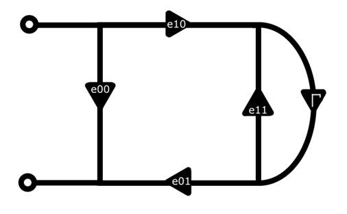
Figure 5: SOL signal flow graph

At this point you may be asking, “How do I measure this reflection coefficient?” The answer is to place it at the end of a transmission line connected to coaxial connectors, and measure it with a VNA. SOL de-embedding can only be done up to the VNA’s coaxial reference. That limits this method since it cannot de-embed test fixtures.
Unknown Standards
TRL
As stated above, TRL stands for Thru-Reflect-Line. A thru is a transmission line that is twice the length of the transmission lines on the test fixture. The reflect is the same length as the test fixture transmission lines with an open or short circuit at the end. The line is a thru with a little extra length. To get the error-box using TRL, the S-parameter data of the standards do not need to be known ahead of time. However, the added length of the line determines the usable bandwidth of the error-box. So, saying that the standards don’t need to be known may be an overstatement.
Equations 3 and 4 show the relationship between the minimum and maximum frequency related to the extra line length.
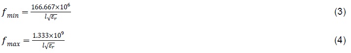
Here, l is the extra length of the transmission line in meters, and εr is the DK given on the PCB material datasheet.
Since there is only limited bandwidth for each line, multiple lines are used to calculate the TRL error-box, and the data from each line is used for its valid bandwidth. Most VNA measurements start at 10 MHz, and it would take a transmission line of length 8.4 m to achieve that! Since that is not practical, the alternative is to use a match as an infinitely long transmission line, and that yields data down to DC, theoretically.
At this point, you are probably thinking “that’s all well and good, but how do I calculate a TRL error-box?” Well, I’m glad that you asked! According to David M. Pozar, the calculation is fairly straight-forward [1]. Start by calculating e-γl with equation 5.

In the equation, Lmn are the S-parameters of the line, and Tmn are the S-parameters of the thru. The choice of sign is made so that the real and imaginary parts of γ are positive. Next, calculate the error-box shown in Figure 6 with the following equations in order.
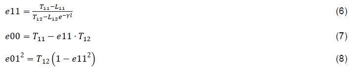 Assume that e01 = e10, and you have found all the error box S-parameters. The derivation for this algorithm and all the juicy details I left out is in David M. Pozar’s Microwave Engineering.
2x-Thru
Here we say “nay” to several standards and “yay” to a one-and-done robust de-embedding technique. A thru alone can achieve the same error box as the TRL technique. Assuming e01 = e10, the signal flow graph of a thru yields two equations.
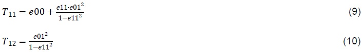
A solution for three unknowns cannot be solved with only two equations; oh no! Have no fear; we use some extra special SI voodoo to capture one of the unknowns indirectly. Bring T12 into the time domain, and calculate its step response. Capture the end of T12 in time by finding its 50% crossing. Next, bring T11 into the time domain, and calculate its step response too. Since the time-of-flight of T11 is twice its position, the end of T12 is the mid-point of T11. All data at and after T11’s mid-point is forced to zero, and the impulse response of this altered data is brought back into the frequency domain; this is e00. Calculate the rest of the error box S-parameters with equations 9 and 10. Take care to ensure that the phase is correct during these calculations. The algorithm for this and a 1x reflect variant are detailed with MATLAB code in the IEEE P370 standard. Interested parties can also contact me directly.
TRL and 2x-Thru methods move the reference plane onto the test fixture. This is an advantage SOL cannot provide. However, TRL and 2x-Thru methods require that the test fixture and standard impedances be identical. When these impedances are different, non-causal DUT S-parameters will result.
In this article, I’ve discussed why de-embedding is important, how to avoid some pit-falls of practical de-embedding, and several de-embedding techniques. I hope you found this article helpful.
[1] D. Pozar, “Electromagnetic Theory”, in Microwave Engineering, 3rd ed, New York, Wiley
[2] Yoon, C. et al, “Design Criteria of Automatic Fixture Removal (AFR) for Asymmetric Fixture De-embedding,” IEEE EMC Symposium, Aug, 2014