
Data centers depend on channels in transmit and receive systems to accurately and efficiently deliver valuable information. A poorly performing device in a channel can cause signal integrity issues and jeopardize the delivery of intelligible data. That makes developing channel devices and interconnects with high signal integrity critical. Testing and identifying the sources of signal integrity issues in a device, then fixing them, is a big challenge.
In a system, signals travel through various kinds of interconnections (e.g., from chip to package, package to board trace, and trace to high-speed connectors). Signal integrity problems arise from the physical nature of interconnecting wires. Unlike a connection line drawn on a schematic, a real wire has resistance, capacitance to ground and other wires, and inductance. At higher frequencies, capacitance and inductance can cause the wire to act as a transmission line, and antenna effects can result in crosstalk and EMI.
Signal integrity problems cause systems to fail or work only intermittently, producing "bad" data. As such, signal integrity issues are particularly important to find early in a design cycle because intermittent failures are very difficult to debug on prototypes.
There are several high-speed design challenges engineers need to consider:
- New standards bring faster speeds and more complex design factors to consider. Complexity is increasing. Today’s radio frequency (RF) and microwave designs require multi-chip modules with more elaborate interconnects and packaging. 5G, for example, requires higher frequencies and broader modulation bandwidth. There is more simulation and measurement data to analyze than ever before. Despite these time-consuming challenges, designers need to accelerate their time to market to stay ahead of the competition.
- Designs need to meet electromagnetic inference and compliance regulations. A system’s ability to operate without introducing an intolerable electromagnetic disturbance is known as electromagnetic compliance (EMC). With increasing data rates in computers, networks, storage, and mobile devices, design engineers need to deal with traditional EMI transmission issues as well as coupling issues with nearby circuit and system components.
- Signal integrity analysis must be performed with accuracy in a reasonable amount of time. Densely-routed boards require hours of engineering time to achieve accurate signal integrity results — including many hours of simulation. Often, designers can only verify small sections of the board at one time. Hybrid simulators add speed and can be used for greater coverage (essentially, with this approach, the connectors are integrated with the board and simulated together using planar and/or 3D EM simulation). However, there is always the question of whether or not the simulation correlates well with measurements.
- Memory designs continue to grow in complexity. Double data rate (DDR) memory designs grow more complex with each new generation. Simulation and test configurations are also growing in complexity, resulting in longer simulation and test setup times. This added complexity makes it challenging to correlate simulation and test data, resulting in less confidence in designs, longer troubleshooting cycles, and missed delivery schedules. Hardware designers working on memory systems must contend with both shrinking timing and voltage margins, and a complex list of compliance measurements to ensure reliable operation.
The traditional approach to finding the root cause of degradation - including delays, ringing, crosstalk, and EMI - is to use analysis techniques like eye diagrams, single pulse response, time-domain reflectometry (TDR), and mixed-mode S-parameters.
Eye diagrams provide you a concise graphical representation of how the channel degrades the signal. An open eye corresponds to minimal signal distortion, and the digital 1 and 0 levels can be clearly distinguished. However, loss and reflections in the system can cause the eye to close, corresponding to distortion of the signal.

Figure 1. Example of an open eye (left) and a closed eye (right).
Single pulse response techniques obtain very complicated data in one pulse, in this way reducing complexity, and then examine how the channel affects the single pulse. It is important to note the rise time of the pulse and the width, which is the bit rate. Refer to figure 2, where the blue line indicates no loss or an ideal scenario, and the purple line indicates a lossy channel. Developing a controlled impedance environment for high-speed digital signals is the best way to guarantee a clean data transmission channel with no bit errors at the receiver. In applications involving signals with gigabit data rates, transmission line properties of the interconnects become critical.
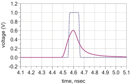
Figure 2. Single-pulse response sends data in one pulse and then examines how the channel affects the single pulse (blue line is the ideal).
Measurements in the time and frequency domains are related. A typical measurement in the time domain is a TDR measurement, which is the measure of the signals reflected from the device’s input as a function of time. In TDR measurements, a fast-rising step edge is sent into the device under test, and the reflected signal measured. TDR identifies impedance discontinuities. The equivalent in the frequency domain is the S11 parameter, which is the ratio of the reflected wave to the incident wave.
The S-parameters of an interconnect, whether measured in the time or the frequency domain, represent a behavioral model of the interconnect. They contain all the information about how a signal entering one port will behave when it exits another port.
S-parameters are saved in touchstone format and shared between simulation and measurement. They are a matrix that shows reflection/transmission characteristics (amplitude/phase) in the frequency domain. S-parameter measurements are critical in high speed digital applications and have increased in importance due to the emergence of gigabit channels in data networks.
A two-port device has four S-parameters. The numbering convention for S-parameters is the first number following the “S” is the port where the signal emerges. The second number is the port where the signal is applied. S21 is a measure of the signal coming out port two relative to the stimulus entering port one. When the numbers are the same (for example, S11), it indicates a reflection measurement. In this case, the input and output ports are the same.
The information provided by four-port differential S-parameters is the principal means to describe the electrical properties of any four-port interconnect. In the complete matrix of measured four-port S-parameters, there is an abundance of data. There are 16 possible combinations of waves going in and out. The 16 S-parameter matrix elements contain everything you need to know about the electrical properties of a differential pair. In cases where more detailed information is necessary, you can use the exported S-parameters as a behavioral model and integrate them directly into circuit simulators in electronic-design automation tools.
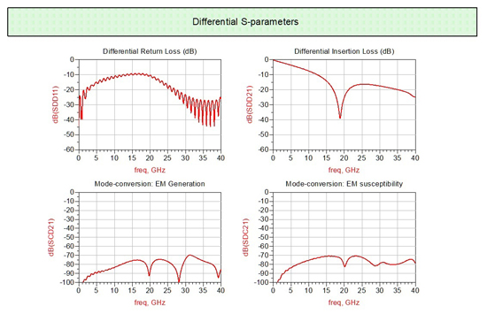
Figure 3. S-parameters allow engineers to gain valuable insight into the performance of high-speed digital interconnects like backplanes, printed circuit boards, cables, connectors, and IC packages.
For today's high-speed boards and ICs, signal integrity is as important to specify as digital functionality or clock speed. Addressing signal integrity issues in densely packed, low power, small form factor circuits is challenging, with perhaps the biggest challenge is discovering when you may be facing signal integrity issues.
The following steps are needed to solve signal integrity problems:
- Simulate the channel
- Identify the root cause of degradation
- Explore design solutions
As part of good design practice, and to ensure the quality of signal transmissions, engineers should consider signal integrity from the time the schematic is drawn until the board passes its final test. By addressing signal integrity problems early, they ensure optimal circuit design that works reliably at a reasonable cost.