
In recent years, the IEEE Electrical Packaging Society (EPS) technical committee for electrical design, modeling, and simulation (TC-EDMS) recognized the need for open-source benchmarks for the simulation tool, verification, and test and measurement solution vendors. The intention is to overcome the obstacles that developers and users of such tools and instruments often encounter and create a growing library of benchmark cases for signal and power integrity challenges.1,2 As of October 2023, there are four published benchmark cases in the repository. This article describes a proposal for a fifth benchmark.
This benchmark is based on the simulation and measurement challenges and test board features that are described in Koether, et al.3,4
Common Test Platform
The overall purpose of this board is to provide the industry with an open-source common test platform that is available to users and can be built by the users if they wish. CAD companies can use the platform to compare simulation tools and setups across different types of simulators from different CAD companies. The platform will allow instrument vendors to refine measurement, calibration, and de-embedding solutions, enabling them to eventually come to a reasonable correlation between simulated and measured values. A common open-source hardware platform would allow various CAD and instrumentation companies to compare their results without sharing confidential details.
The intended use of this benchmark test board is to facilitate the investigation of three areas: to analyze the impact of probe-tip coupling in wafer probe calibrations and measurements; to investigate the impact of via coupling within the device under test; and to better understand the spatial effects associated with large via arrays in low impedance power distribution networks. The associated pieces in a power distribution network (PDN) are illustrated in Figure 1.
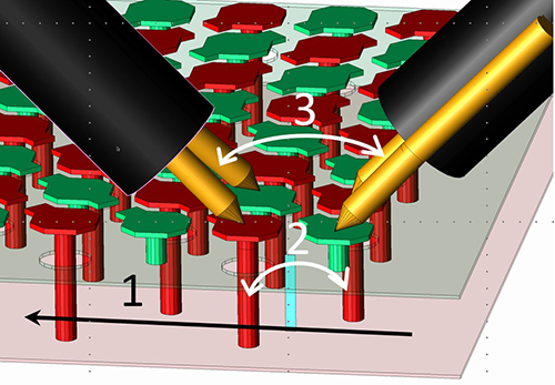
Figure 1. 3D rendering of two single-ended wafer probes touching down on the corner of a large via array, illustrating the three possible areas of investigation: 1) probe-tip coupling, 2) via-loop coupling, and 3) spatial effects.3
This benchmark board is not intended for high-frequency modeling, high-frequency correlation, or high-frequency laminate characterization. This board is designed for wafer probe connections, not for direct coaxial connection.
Description of the Board
The board has six metal layers and can be built with low-cost foil construction lamination and with low-cost laminate materials. The same stackup can also be built with different laminates, not only with the one described here. Note that some of the power-ground laminates, especially the very thin ones, may require a sequential lamination process required by the laminate itself.
The 10 × 7.5 in. board is divided into six identical rectangular areas or sections, as shown in Figure 2. As described in detail later, each rectangular section has full planes within and only within their own boundaries, on all of their four internal core layers. The TOP and BOTTOM layers are pad only.
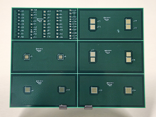
Figure 2. Front-view photo of the manufactured benchmark board as described in this article.
Stackup
The default board stackup, used for the first build, is shown on a PCB fab vendor drawing in Figure 3. Within practical limits, the same board construction can be built not only with different laminates, but also with different stackup-number targets. Some of the main stackup option considerations are summarized later.
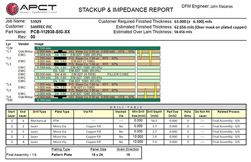
Figure 3. Typical stackup and drill definitions of the board. The nominal dimensions and materials are shown for the first build.
Materials
The first boards were built with the same kind of laminate throughout all of the layers, EMC EM-827, which is considered to be equivalent to Isola 370HR, the popular low-frequency laminate. Figure 4 shows the major mechanical and electrical properties of the laminate.

Figure 4. EM-827 material properties.
Construction, Stackup, and Material Options
As will be shown later, there are plated through hole arrays in two of the sections and blind via arrays in three of the sections. One section has various combinations of reference vias, both blind vias and through vias. There are no buried vias in the board and no sequential lamination is required, unless a stackup variant is used with very different core laminates, either much thinner or much thicker. In the former, the laminate itself may require sequential processing; in the latter, reaching layer 3 from the top or layer 4 from the bottom may not work with blind vias.
The thin outer prepreg allows us to keep the low-cost foil construction and use laser-drilled blind vias as long as the smallest-pitch via array can accommodate the L1-L3 and L6-L4 skip vias, which normally would be limited by the maximum allowed aspect ratio.
The current construction allows stackup variants with thinner L2-L3 and L4-L5 cores and/or heavier copper on those cores. In addition to different copper thicknesses, different copper types, and/or different roughness values can also be used, though roughness is usually considered of secondary importance in power distribution networks. For easy comparison across different builds, the overall board thickness can be held constant while using different laminate thickness and copper weight options by adjusting the thickness of the middle prepreg accordingly. Alternately, the total board thickness can also be made different on purpose if the user wants to study and correlate via structures reaching to various depths.
Board Finish and Silkscreen
Though this board does not assume any soldered assembly, and in general it may have very little direct influence on the power distribution performance of the board, passivation of exposed copper is still recommended. The board was built with a flash gold surface finish. The exposed dielectric on the board surface is covered by the customary green solder mask; again, since this board is primarily for lower-frequency PDN tests, the solder mask has very little influence on the performance in that frequency range. To help locate various structures during measurements, the board has silkscreen on the top and bottom. In the board file, each group of vias has a reference designator, and the vias have pin IDs assigned.
Finally, the surface has a thieving pattern that covers all unused areas. The thieving pattern for this board is small diamond shapes, but as long as the size of each copper feature is much less than the wavelength, the size and shape will not matter. Figure 5 illustrates these features.

Figure 5. Illustration of gold surface finish, green solder mask, silk screen for via arrays and reference patterns, and thieving pattern on the outer layers of the board.
Layout
The fab drawing image in Figure 6 shows that within the 10 × 7.5 in. envelope, there are six sections with identical plane sizes on L2, L3, L4, and L5. The planes in each section are 4.925 × 2.425 in. in size. The six sections, numbered clockwise, are referred to as Sections 1 through 6, as shown in Figure 7.

Figure 6. Fab drawing detail showing the outer dimensions (10 x 7.5 in.).
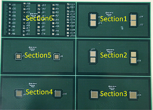
Figure 7. Top board view displaying the numbering of the six sections.
Sections 1 through 5 have 8 × 8 via arrays with different via pitches, different connections, and different technologies. Section 6 is a reference section, with two or four vias using the plane connections and via technology that we have in Sections 1 through 5. Figure 8 shows the top view of a 1 mm plated through hole array. Pin A1 is connected to GND in all arrays; from there, the pins follow a checker-board pattern and alternate between power and ground.
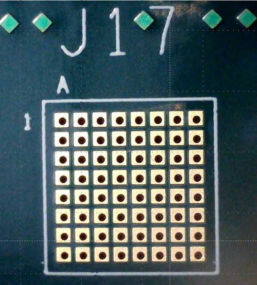
Figure 8. 8 x 8 via array on Sections 1 through 5.
Overview of Sections
While each section serves a useful purpose, this document focuses on two sections, Section 2 and its corresponding reference features in Section 6.
Section 1
In Section 1, all four via arrays, with reference designators J21, J22, J23, and J24, are connected to both plane cavities, thus allowing us to look at vertical attenuation patterns in PDNs (see Figure 9). Note that in this section, all four via arrays are interconnected together through the planes.

Figure 9. Top view of Section 1, holding four 1 mm plated through hole arrays.
Section 2
As shown in Figure 10, Section 2 has four 8 x 8 via arrays: J17, J18, J19, and J20. J17 and J18 connect to the L2-L3 plane cavity, whereas J19 and J20 connect to the L4-L5 plane cavity. The via pitch is 1 mm (approximately 40 mil), same as in Section 1; the padstack for the through via is captured in Figure 11. Note that because all four arrays use through holes and all four arrays are accessible from both the top and bottom side, the two sets of two via arrays are not connected together.
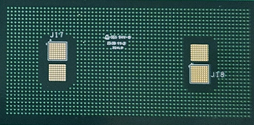
Figure 10. Top view of Section 2, holding four 1 mm plated through hole arrays.
Figure 11. Via and padstack definition of the 1 mm plated through hole arrays.
Sections 3 Through 5
These three sections use blind vias. Each section has four via arrays — two on the top, connecting to L2 and L3, and two on the bottom, connecting to L4 and L5. Section 3 uses 1.27 mm (50 mil) via pitch, whereas the via pitch in Sections 4 and 5 is 1 mm and 0.8 mm, respectively; see Figure 12.

Figure 12. Top view of Sections 3, 4, and 5.
Because the blind vias do not go through the board vertically, we can place the via arrays at the same X-Y location. Note that as long as we keep the stackup symmetric and balanced, the two via arrays on the top and on the bottom should behave identically. The reason for the duplication is that it allows us to do redundant measurements.
Section 6, Reference
Section 6 has the various via types, sizes, and pitches that are used on Sections 1 through 5 in groups of two and four vias, making it simpler and easier to measure and correlate. Also, most of the reference vias connect intentionally to the same planes, which allows us to analyze shorter and longer via loops without the added complexity of a plane cavity. As shown in Figure 13, the reference vias in Section 6 are arranged in five columns, corresponding to the five sections with different via arrays. Figure 14 shows the connectivity of each of the nine reference via groups.
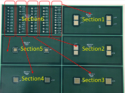
Figure 13. Five columns of reference vias in Section 6.
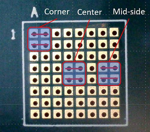
Figure 14. Connectivity in the reference via groups referring to Section 2.
Focus Area
Section 2 offers the opportunity to probe via arrays that are connected to one plane cavity only. Moreover, the through vias allow us to probe in various configurations. To name a few obvious choices: we can probe at the selected via pair from top to bottom, and at adjacent or more distant neighbor via pairs from the same side, either top or bottom. The spatial effect can be looked at by probing the structure at different locations; for instance, at the corner, center, and at the mid-point of a side. The suggested locations in Figure 15 also provide the possibility to get transfer parameters between more distant locations.

Figure 15. Suggested port locations for Section 2 J17 measurements and simulations.
If we probe power-ground vias in the via arrays with nothing attached to the board, we actually probe an open-terminated plane cavity that represents capacitive reactance at low frequencies. At high frequencies, where the modal resonances of the planes develop, we could also collect information about the dielectric properties. If we limit ourselves to frequencies below the modal resonances, we need a shorted structure so that we can assess the resistance and inductance of the structure. We can solder a shorting plane over the second via array on the planes, in this case, J18, but it may require a professional BGA soldering station to do so properly and repeatedly. Alternatively, we can easily create removable shorts by clamping a carefully flattened copper sheet, cut to the proper size, over the entire via array of J18. To make sure that the connection is repeatable, we can apply silver paste on the shorting copper sheet.
To complement the data that we can collect on the via arrays, the reference via groups offer further correlation opportunities, as several of them create a directly shorted conductive path without the need to go through the plane cavity and the second via array to create a closed loop. For instance, we can measure the via group in J84 in different configurations, preferably with the same port orientation and port assignment that we use for the three locations at J17 (see Figure 16). The four vias in J84 can be considered as a cutout from J17 at the three selected locations, with the only difference being that all four vias are connected to L2, shorting them together. Even though we have only four vias in the group, this structure, just like several of the other reference via groups, offers a large number of possible permutations to simulate and/or to measure. Note that via group J90 similarly connects all four vias to the same plane, but it is L3 instead of L2.
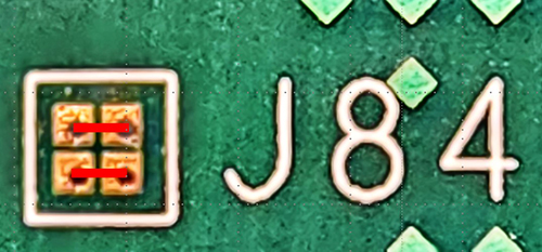
Figure 16. Suggested port orientation for measurements and simulations in Section 6 J84.
Summary
Eventually, when the design becomes open-source, the goal is to make available the following material:
- Native Allegro board file, Gerber files, ODB++ files, and IPC2581 files
- Schematics file in native Cadence format, as well as in industry standard IPC-356 and PDF formats
- Material and stackup definitions of the manufactured boards
- Sample measurement data on Section 2 and Section 6
- Sample simulation data on Section 2 and Section 6.
The documentation will enable users to fabricate the benchmark boards themselves, either in its default construction or in any variant of it. The default benchmark board may also become available for purchase.
In addition to the documentation, script(s) to analyze, compare, and post-process measured and simulated data may also become available in the future.
Acknowledgements
The authors wish to thank Heidi Barnes and every member of the IEEE TC-EDMS Packaging Benchmarks Committee as well as Patrick Davis and Jonathon Hendren of Cadence; Richard Zai of PacketMicro; and Jean-Remy Bonnefoy, Steve Duzan, and Julia Van Burger of Samtec for their help and assistance with this project.
REFERENCES
- IEEE EPS TC-EDMS Packaging Benchmark Suite, 2021. [Online]. Available: https://packaging-benchmarks.org.
- H. Barnes, et al., “The IEEE EPS Packaging Benchmark Suite,” IEEE 2022.
- E. Koether, et al., “3D Connection Artifacts in PDN Measurements,” DesignCon 2023.
- E. Koether, et al, “Impact of Finite Interconnect Impedance including Spatial and Domain Comparison of PDN Characterization,” to be published at DesignCon 2024.